
Datasheet


Table Of Contents
- 1 Digital Media System-on-Chip (DMSoC)
- Table of Contents
- 2 Revision History
- 3 Device Overview
- 3.1 Device Characteristics
- 3.2 Device Compatibility
- 3.3 ARM Subsystem
- 3.3.1 ARM926EJ-S RISC CPU
- 3.3.2 CP15
- 3.3.3 MMU
- 3.3.4 Caches and Write Buffer
- 3.3.5 Tightly Coupled Memory (TCM)
- 3.3.6 Advanced High-Performance Bus (AHB)
- 3.3.7 Embedded Trace Macrocell (ETM) and Embedded Trace Buffer (ETB)
- 3.3.8 ARM Memory Mapping
- 3.3.9 Peripherals
- 3.3.10 PLL Controller (PLLC)
- 3.3.11 Power and Sleep Controller (PSC)
- 3.3.12 ARM Interrupt Controller (AINTC)
- 3.3.13 System Module
- 3.3.14 Power Management
- 3.4 DSP Subsystem
- 3.5 Memory Map Summary
- 3.6 Pin Assignments
- 3.7 Terminal Functions
- 3.8 Device Support
- 3.9 Documentation Support
- 3.10 Community Resources
- 4 Device Configurations
- 4.1 System Module Registers
- 4.2 Power Considerations
- 4.3 Clock Considerations
- 4.4 Boot Sequence
- 4.5 Configurations At Reset
- 4.6 Configurations After Reset
- 4.7 Multiplexed Pin Configurations
- 4.7.1 Pin Muxing Selection At Reset
- 4.7.2 Pin Muxing Selection After Reset
- 4.7.3 Pin Multiplexing Details
- 4.7.3.1 PCI, HPI, EMIFA, and ATA Pin Muxing
- 4.7.3.2 PWM Signal Muxing
- 4.7.3.3 TSIF0 Input Signal Muxing (Serial/Parallel)
- 4.7.3.4 TSIF0 Output Signal Muxing (Serial/Parallel)
- 4.7.3.5 TSIF1 Input Signal Muxing (Serial Only)
- 4.7.3.6 TSIF1 Output Signal Muxing (Serial Only)
- 4.7.3.7 CRGEN Signal Muxing
- 4.7.3.8 UART0 Pin Muxing
- 4.7.3.9 UART1 Pin Muxing
- 4.7.3.10 UART2 Pin Muxing
- 4.7.3.11 ARM/DSP Communications Interrupts
- 4.7.3.12 Emulation Control
- 4.8 Debugging Considerations
- 5 System Interconnect
- 6 Device Operating Conditions
- 7 Peripheral Information and Electrical Specifications
- 7.1 Parameter Information
- 7.2 Recommended Clock and Control Signal Transition Behavior
- 7.3 Power Supplies
- 7.4 External Clock Input From DEV_MXI/DEV_CLKIN and AUX_MXI/AUX_CLKIN Pins
- 7.5 Clock PLLs
- 7.6 Enhanced Direct Memory Access (EDMA3) Controller
- 7.7 Reset
- 7.8 Interrupts
- 7.9 External Memory Interface (EMIF)
- 7.10 DDR2 Memory Controller
- 7.10.1 DDR2 Memory Controller Electrical Data/Timing
- 7.10.2 DDR2 Interface
- 7.10.2.1 DDR2 Interface Schematic
- 7.10.2.2 Compatible JEDEC DDR2 Devices
- 7.10.2.3 PCB Stackup
- 7.10.2.4 Placement
- 7.10.2.5 DDR2 Keep Out Region
- 7.10.2.6 Bulk Bypass Capacitors
- 7.10.2.7 High-Speed Bypass Capacitors
- 7.10.2.8 Net Classes
- 7.10.2.9 DDR2 Signal Termination
- 7.10.2.10 VREF Routing
- 7.10.2.11 DDR2 CK and ADDR_CTRL Routing
- 7.11 Video Port Interface (VPIF)
- 7.12 Transport Stream Interface (TSIF)
- 7.13 Clock Recovery Generator (CRGEN)
- 7.14 Video Data Conversion Engine (VDCE)
- 7.15 Peripheral Component Interconnect (PCI)
- 7.16 Ethernet MAC (EMAC)
- 7.17 Management Data Input/Output (MDIO)
- 7.18 Host-Port Interface (HPI) Peripheral
- 7.19 USB 2.0 [see Note]
- 7.20 ATA Controller
- 7.21 VLYNQ
- 7.22 Multichannel Audio Serial Port (McASP0/1) Peripherals
- 7.23 Serial Peripheral Interface (SPI)
- 7.24 Universal Asynchronouse Receiver/Transmitter (UART)
- 7.25 Inter-Integrated Circuit (I2C)
- 7.26 Pulse Width Modulator (PWM)
- 7.27 Timers
- 7.28 General-Purpose Input/Output (GPIO)
- 7.29 IEEE 1149.1 JTAG
- 8 Mechanical Packaging and Orderable Information
TMS320DM6467T
www.ti.com
SPRS605C –JULY 2009–REVISED JUNE 2012
7.20 ATA Controller
The ATA peripheral supports the following features:
• PIO, multiword DMA, and Ultra ATA 33/66/100
• Up to mode 4 timings on PIO mode
• Up to mode 2 timings on multiword DMA
• Up to mode 5 timings on Ultra ATA
• Programmable timing parameters
• Supports TrueIDE mode for Compact Flash
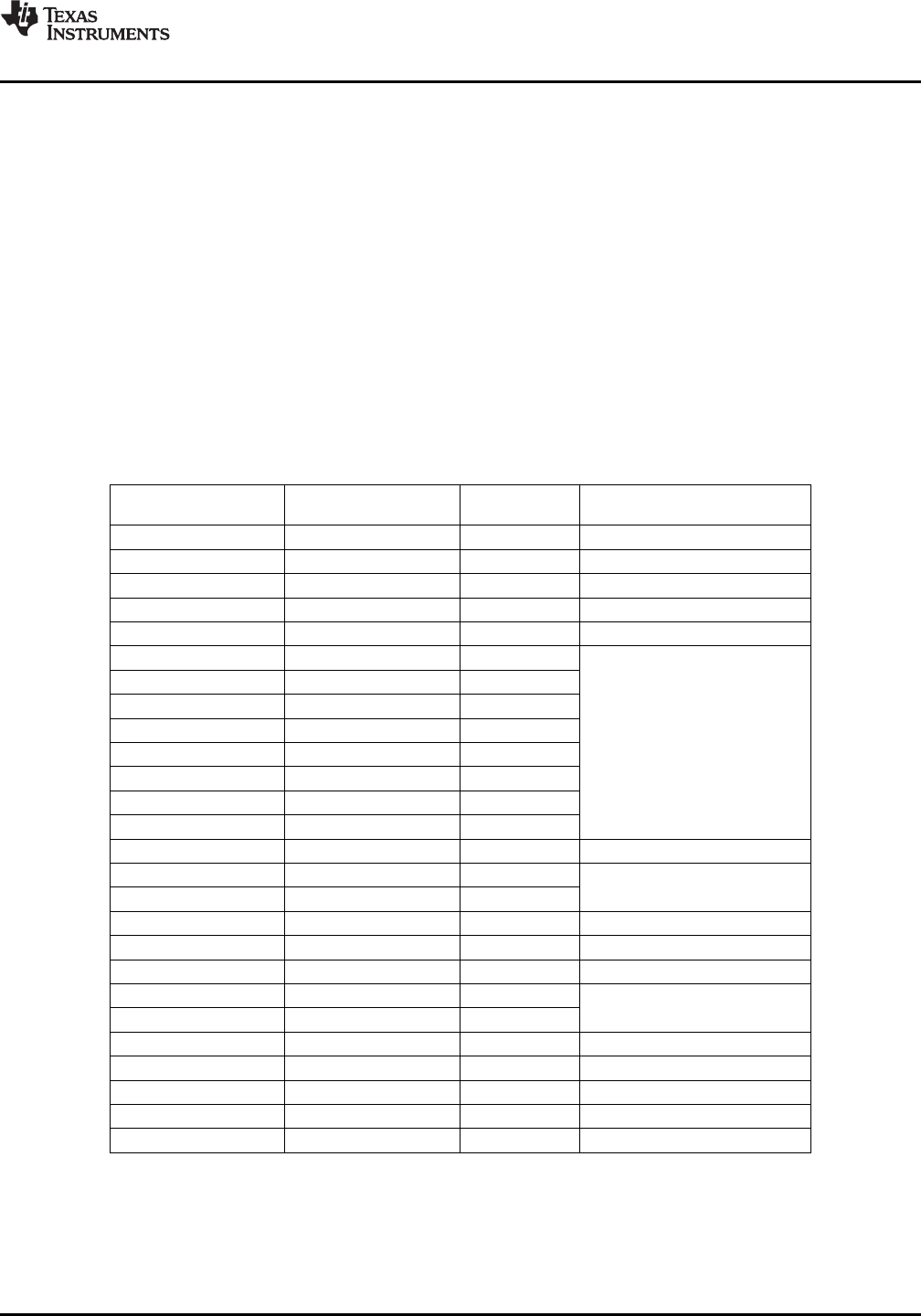
7.20.1 ATA Bus Master Memory Map
The ATA Controller supports multiword DMA transfers between external IDE/ATAPI devices and a system
memory bus interface. Table 7-88 shows the memory map for the ATA DMA engine.
Table 7-88. ATA DMA Master Memory Map
SIZE
START ADDRESS END ADDRESS ATA DMA ACCESS
(BYTES)
0x0000 0000 0x0FFF FFFF 256M Reserved
0x1000 0000 0x1000 FFFF 64K Reserved
0x1001 0000 0x1001 3FFF 16K ARM RAM 0 (Data)
0x1001 4000 0x1001 7FFF 16K ARM RAM 1 (Data)
0x1001 8000 0x1001 FFFF 32K ARM ROM (Data)
0x1002 0000 0x10FF FFFF 16256K
0x1100 0000 0x113F FFFF 4M
0x1140 0000 0x114F FFFF 1M
0x1150 0000 0x115F FFFF 1M
Reserved
0x1160 0000 0x116F FFFF 1M
0x1170 0000 0x117F FFFF 1M
0x1180 0000 0x1180 FFFF 64K
0x1181 0000 0x1181 7FFF 32K
0x1181 8000 0x1183 7FFF 128K C64x+ L2 RAM/Cache
0x1183 8000 0x118F FFFF 800K
Reserved
0x1190 0000 0x11DF FFFF 5M
0x11E0 0000 0x11E0 7FFF 32K C64x+ L1P RAM/Cache
0x11E0 8000 0x11EF FFFF 992K Reserved
0x11F0 0000 0x11F0 7FFF 32K C64x+ L1D RAM/Cache
0x11F0 8000 0x11FF FFFF 992K
Reserved
0x1200 0000 0x4BFF FFFF 928M
0x4C00 0000 0x4FFF FFFF 64M VLYNQ (Remote Data)
0x5000 0000 0x7FFF FFFF 768M Reserved
0x8000 0000 0x9FFF FFFF 512M DDR2 Memory Controller
0xA000 0000 0xBFFF FFFF 512M Reserved
0xC000 0000 0xFFFF FFFF 1G Reserved
Copyright © 2009–2012, Texas Instruments Incorporated Peripheral Information and Electrical Specifications 279
Submit Documentation Feedback
Product Folder Link(s): TMS320DM6467T