
Datasheet


Table Of Contents
- 1 Digital Media System-on-Chip (DMSoC)
- Table of Contents
- 2 Revision History
- 3 Device Overview
- 3.1 Device Characteristics
- 3.2 Device Compatibility
- 3.3 ARM Subsystem
- 3.3.1 ARM926EJ-S RISC CPU
- 3.3.2 CP15
- 3.3.3 MMU
- 3.3.4 Caches and Write Buffer
- 3.3.5 Tightly Coupled Memory (TCM)
- 3.3.6 Advanced High-Performance Bus (AHB)
- 3.3.7 Embedded Trace Macrocell (ETM) and Embedded Trace Buffer (ETB)
- 3.3.8 ARM Memory Mapping
- 3.3.9 Peripherals
- 3.3.10 PLL Controller (PLLC)
- 3.3.11 Power and Sleep Controller (PSC)
- 3.3.12 ARM Interrupt Controller (AINTC)
- 3.3.13 System Module
- 3.3.14 Power Management
- 3.4 DSP Subsystem
- 3.5 Memory Map Summary
- 3.6 Pin Assignments
- 3.7 Terminal Functions
- 3.8 Device Support
- 3.9 Documentation Support
- 3.10 Community Resources
- 4 Device Configurations
- 4.1 System Module Registers
- 4.2 Power Considerations
- 4.3 Clock Considerations
- 4.4 Boot Sequence
- 4.5 Configurations At Reset
- 4.6 Configurations After Reset
- 4.7 Multiplexed Pin Configurations
- 4.7.1 Pin Muxing Selection At Reset
- 4.7.2 Pin Muxing Selection After Reset
- 4.7.3 Pin Multiplexing Details
- 4.7.3.1 PCI, HPI, EMIFA, and ATA Pin Muxing
- 4.7.3.2 PWM Signal Muxing
- 4.7.3.3 TSIF0 Input Signal Muxing (Serial/Parallel)
- 4.7.3.4 TSIF0 Output Signal Muxing (Serial/Parallel)
- 4.7.3.5 TSIF1 Input Signal Muxing (Serial Only)
- 4.7.3.6 TSIF1 Output Signal Muxing (Serial Only)
- 4.7.3.7 CRGEN Signal Muxing
- 4.7.3.8 UART0 Pin Muxing
- 4.7.3.9 UART1 Pin Muxing
- 4.7.3.10 UART2 Pin Muxing
- 4.7.3.11 ARM/DSP Communications Interrupts
- 4.7.3.12 Emulation Control
- 4.8 Debugging Considerations
- 5 System Interconnect
- 6 Device Operating Conditions
- 7 Peripheral Information and Electrical Specifications
- 7.1 Parameter Information
- 7.2 Recommended Clock and Control Signal Transition Behavior
- 7.3 Power Supplies
- 7.4 External Clock Input From DEV_MXI/DEV_CLKIN and AUX_MXI/AUX_CLKIN Pins
- 7.5 Clock PLLs
- 7.6 Enhanced Direct Memory Access (EDMA3) Controller
- 7.7 Reset
- 7.8 Interrupts
- 7.9 External Memory Interface (EMIF)
- 7.10 DDR2 Memory Controller
- 7.10.1 DDR2 Memory Controller Electrical Data/Timing
- 7.10.2 DDR2 Interface
- 7.10.2.1 DDR2 Interface Schematic
- 7.10.2.2 Compatible JEDEC DDR2 Devices
- 7.10.2.3 PCB Stackup
- 7.10.2.4 Placement
- 7.10.2.5 DDR2 Keep Out Region
- 7.10.2.6 Bulk Bypass Capacitors
- 7.10.2.7 High-Speed Bypass Capacitors
- 7.10.2.8 Net Classes
- 7.10.2.9 DDR2 Signal Termination
- 7.10.2.10 VREF Routing
- 7.10.2.11 DDR2 CK and ADDR_CTRL Routing
- 7.11 Video Port Interface (VPIF)
- 7.12 Transport Stream Interface (TSIF)
- 7.13 Clock Recovery Generator (CRGEN)
- 7.14 Video Data Conversion Engine (VDCE)
- 7.15 Peripheral Component Interconnect (PCI)
- 7.16 Ethernet MAC (EMAC)
- 7.17 Management Data Input/Output (MDIO)
- 7.18 Host-Port Interface (HPI) Peripheral
- 7.19 USB 2.0 [see Note]
- 7.20 ATA Controller
- 7.21 VLYNQ
- 7.22 Multichannel Audio Serial Port (McASP0/1) Peripherals
- 7.23 Serial Peripheral Interface (SPI)
- 7.24 Universal Asynchronouse Receiver/Transmitter (UART)
- 7.25 Inter-Integrated Circuit (I2C)
- 7.26 Pulse Width Modulator (PWM)
- 7.27 Timers
- 7.28 General-Purpose Input/Output (GPIO)
- 7.29 IEEE 1149.1 JTAG
- 8 Mechanical Packaging and Orderable Information
USB_V
SSREF
USB_R1
USB
10K ±1%Ω
(A)
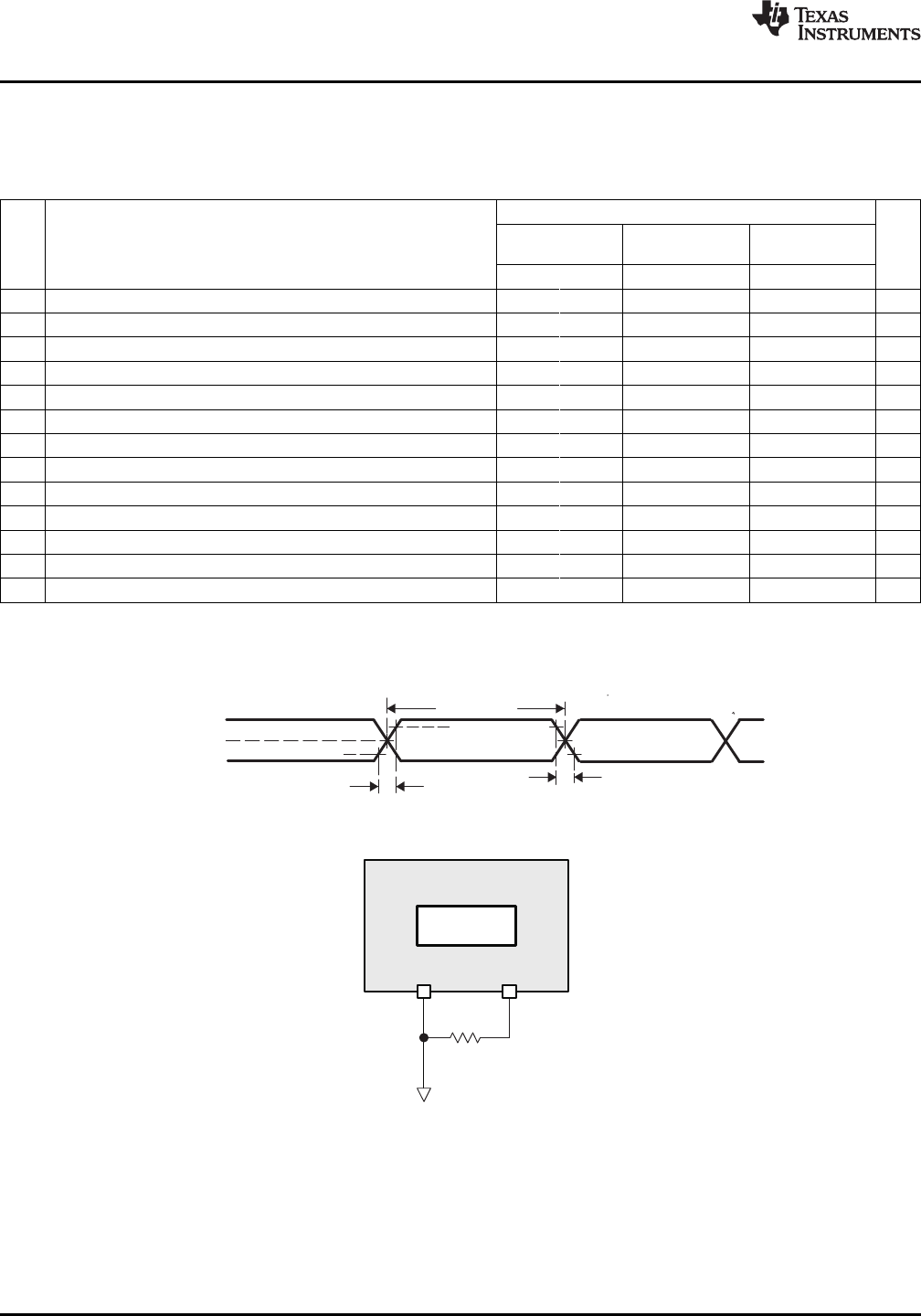
A.Placethe10K Ω ±1%asclosetothedeviceaspossible.
t
r
t
f
V
CRS
90% V
OH
10% V
OL
USB_DN
USB_DP
t
per
−
t
jr
TMS320DM6467T
SPRS605C –JULY 2009–REVISED JUNE 2012
www.ti.com
7.19.4 USB2.0 Electrical Data/Timing
Table 7-87. Switching Characteristics Over Recommended Operating Conditions for USB2.0 (see
Figure 7-62)
-1G
LOW SPEED FULL SPEED HIGH SPEED
NO. PARAMETER UNIT
1.5 Mbps 12 Mbps 480 Mbps
MIN MAX MIN MAX MIN MAX
1 t
r(D)
Rise time, USB_DP and USB_DN signals
(1)
75 300 4 20 0.5 ns
2 t
f(D)
Fall time, USB_DP and USB_DN signals
(1)
75 300 4 20 0.5 ns
3 t
rfM
Rise/Fall time, matching
(2)
80 125 90 111.11 – – %
4 V
CRS
Output signal cross-over voltage
(1)
1.3 2 1.3 2 – – V
5 t
jr(source)NT
Source (Host) Driver jitter, next transition 2 2
(3)
ns
t
jr(FUNC)NT
Function Driver jitter, next transition 25 2
(3)
ns
6 t
jr(source)PT
Source (Host) Driver jitter, paired transition
(4)
1 1
(3)
ns
t
jr(FUNC)PT
Function Driver jitter, paired transition 10 1
(3)
ns
7 t
w(EOPT)
Pulse duration, EOP transmitter 1250 1500 160 175 – – ns
8 t
w(EOPR)
Pulse duration, EOP receiver 670 82 – ns
9 t
(DRATE)
Data Rate 1.5 12 480 Mb/s
10 Z
DRV
Driver Output Resistance – – 28 49.5 40.5 49.5 Ω
11 USB_R1 USB reference resistor 9.9 10.1 9.9 10.1 9.9 10.1 kΩ
(1) Low Speed: C
L
= 200 pF, Full Speed: C
L
= 50 pF, High Speed: C
L
= 50 pF
(2) t
RFM
= (t
r
/t
f
) x 100. [Excluding the first transaction from the Idle state.]
(3) For more detailed information, see the Universal Serial Bus Specification Revision 2.0, Chapter 7. Electrical.
(4) t
jr
= t
px(1)
- t
px(0)
Figure 7-62. USB2.0 Integrated Transceiver Interface Timing
Figure 7-63. USB Reference Resistor Routing
278 Peripheral Information and Electrical Specifications Copyright © 2009–2012, Texas Instruments Incorporated
Submit Documentation Feedback
Product Folder Link(s): TMS320DM6467T