
Datasheet


Table Of Contents
- 1 Digital Media System-on-Chip (DMSoC)
- Table of Contents
- 2 Revision History
- 3 Device Overview
- 3.1 Device Characteristics
- 3.2 Device Compatibility
- 3.3 ARM Subsystem
- 3.3.1 ARM926EJ-S RISC CPU
- 3.3.2 CP15
- 3.3.3 MMU
- 3.3.4 Caches and Write Buffer
- 3.3.5 Tightly Coupled Memory (TCM)
- 3.3.6 Advanced High-Performance Bus (AHB)
- 3.3.7 Embedded Trace Macrocell (ETM) and Embedded Trace Buffer (ETB)
- 3.3.8 ARM Memory Mapping
- 3.3.9 Peripherals
- 3.3.10 PLL Controller (PLLC)
- 3.3.11 Power and Sleep Controller (PSC)
- 3.3.12 ARM Interrupt Controller (AINTC)
- 3.3.13 System Module
- 3.3.14 Power Management
- 3.4 DSP Subsystem
- 3.5 Memory Map Summary
- 3.6 Pin Assignments
- 3.7 Terminal Functions
- 3.8 Device Support
- 3.9 Documentation Support
- 3.10 Community Resources
- 4 Device Configurations
- 4.1 System Module Registers
- 4.2 Power Considerations
- 4.3 Clock Considerations
- 4.4 Boot Sequence
- 4.5 Configurations At Reset
- 4.6 Configurations After Reset
- 4.7 Multiplexed Pin Configurations
- 4.7.1 Pin Muxing Selection At Reset
- 4.7.2 Pin Muxing Selection After Reset
- 4.7.3 Pin Multiplexing Details
- 4.7.3.1 PCI, HPI, EMIFA, and ATA Pin Muxing
- 4.7.3.2 PWM Signal Muxing
- 4.7.3.3 TSIF0 Input Signal Muxing (Serial/Parallel)
- 4.7.3.4 TSIF0 Output Signal Muxing (Serial/Parallel)
- 4.7.3.5 TSIF1 Input Signal Muxing (Serial Only)
- 4.7.3.6 TSIF1 Output Signal Muxing (Serial Only)
- 4.7.3.7 CRGEN Signal Muxing
- 4.7.3.8 UART0 Pin Muxing
- 4.7.3.9 UART1 Pin Muxing
- 4.7.3.10 UART2 Pin Muxing
- 4.7.3.11 ARM/DSP Communications Interrupts
- 4.7.3.12 Emulation Control
- 4.8 Debugging Considerations
- 5 System Interconnect
- 6 Device Operating Conditions
- 7 Peripheral Information and Electrical Specifications
- 7.1 Parameter Information
- 7.2 Recommended Clock and Control Signal Transition Behavior
- 7.3 Power Supplies
- 7.4 External Clock Input From DEV_MXI/DEV_CLKIN and AUX_MXI/AUX_CLKIN Pins
- 7.5 Clock PLLs
- 7.6 Enhanced Direct Memory Access (EDMA3) Controller
- 7.7 Reset
- 7.8 Interrupts
- 7.9 External Memory Interface (EMIF)
- 7.10 DDR2 Memory Controller
- 7.10.1 DDR2 Memory Controller Electrical Data/Timing
- 7.10.2 DDR2 Interface
- 7.10.2.1 DDR2 Interface Schematic
- 7.10.2.2 Compatible JEDEC DDR2 Devices
- 7.10.2.3 PCB Stackup
- 7.10.2.4 Placement
- 7.10.2.5 DDR2 Keep Out Region
- 7.10.2.6 Bulk Bypass Capacitors
- 7.10.2.7 High-Speed Bypass Capacitors
- 7.10.2.8 Net Classes
- 7.10.2.9 DDR2 Signal Termination
- 7.10.2.10 VREF Routing
- 7.10.2.11 DDR2 CK and ADDR_CTRL Routing
- 7.11 Video Port Interface (VPIF)
- 7.12 Transport Stream Interface (TSIF)
- 7.13 Clock Recovery Generator (CRGEN)
- 7.14 Video Data Conversion Engine (VDCE)
- 7.15 Peripheral Component Interconnect (PCI)
- 7.16 Ethernet MAC (EMAC)
- 7.17 Management Data Input/Output (MDIO)
- 7.18 Host-Port Interface (HPI) Peripheral
- 7.19 USB 2.0 [see Note]
- 7.20 ATA Controller
- 7.21 VLYNQ
- 7.22 Multichannel Audio Serial Port (McASP0/1) Peripherals
- 7.23 Serial Peripheral Interface (SPI)
- 7.24 Universal Asynchronouse Receiver/Transmitter (UART)
- 7.25 Inter-Integrated Circuit (I2C)
- 7.26 Pulse Width Modulator (PWM)
- 7.27 Timers
- 7.28 General-Purpose Input/Output (GPIO)
- 7.29 IEEE 1149.1 JTAG
- 8 Mechanical Packaging and Orderable Information
TMS320DM6467T
www.ti.com
SPRS605C –JULY 2009–REVISED JUNE 2012
7.19.3 USB2.0 Peripheral Register Description(s)
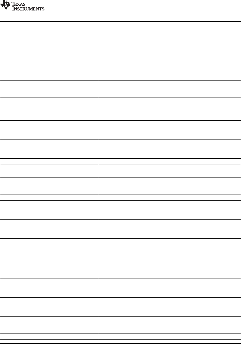
Table 7-86 shows the USB perripheral register memory mapping.
Table 7-86. USB2.0 Registers
HEX ADDRESS
ACRONYM REGISTER NAME
RANGE
0x01C6 4000 REVR Revision Register
0x01C6 4004 CTRLR Control Register
0x01C6 4008 STATR Status Register
0x01C6 400C - Reserved
–
0x01C6 400F
0x01C6 4010 RNDISR RNDIS Register
0x01C6 4014 AUTOREQ Auto Request Register
0x01C6 4018 - Reserved
–
0x01C6 401F
0x01C6 4020 INTSRCR USB Interrupt Source Register
0x01C6 4024 INTSETR USB Interrupt Source Set Register
0x01C6 4028 INTCLRR USB Interrupt Source Clear Register
0x01C6 402C INTMSKR USB Interrupt Mask Register
0x01C6 4030 INTMSKSETR USB Interrupt Mask Set Register
0x01C6 4034 INTMSKCLRR USB Interrupt Mask Clear Register
0x01C6 4038 INTMASKEDR USB Interrupt Source Masked Register
0x01C6 403C EOIR USB End of Interrupt Register
0x01C6 4040 INTVECTR USB Interrupt Vector Register
0x01C6 4044 - Reserved
–
0x01C6 407F
0x01C6 4080 TCPPICR TX CPPI Control Register
0x01C6 4084 TCPPITDR TX CPPI Teardown Register
0x01C6 4088 TCPPIEOIR TX CPPI DMA Controller End of Interrupt Register
0x01C6 408C TCPPIIVECTR TX CPPI DMA Controller Interrupt Vector Register
0x01C6 4090 TCPPIMSKSR TX CPPI Masked Status Register
0x01C6 4094 TCPPIRAWSR TX CPPI Raw Status Register
0x01C6 4098 TCPPIIENSETR TX CPPI Interrupt Enable Set Register
0x01C6 409C TCPPIIENCLRR TX CPPI Interrupt Enable Clear Register
0x01C6 40A0 - Reserved
–
0x01C6 40BF
0x01C6 40C0 RCPPICR RX CPPI Control Register
0x01C6 40C4 - Reserved
–
0x01C6 40CF
0x01C6 40D0 RCPPIMSKSR RX CPPI Masked Status Register
0x01C6 40D4 RCPPIRAWSR RX CPPI Raw Status Register
0x01C6 40D8 RCPPIENSETR RX CPPI Interrupt Enable Set Register
0x01C6 40DC RCPPIIENCLRR RX CPPI Interrupt Enable Clear Register
0x01C6 40E0 RBUFCNT0 RX Buffer Count 0 Register
0x01C6 40E4 RBUFCNT1 RX Buffer Count 1 Register
0x01C6 40E8 RBUFCNT2 RX Buffer Count 2 Register
0x01C6 40EC RBUFCNT3 RX Buffer Count 3 Register
0x01C6 40F0 - Reserved
–
0x01C6 40FF
TX/RX CCPI Channel 0 State Block
0x01C6 4100 TCPPIDMASTATEW0 TX CPPI DMA State Word 0
Copyright © 2009–2012, Texas Instruments Incorporated Peripheral Information and Electrical Specifications 271
Submit Documentation Feedback
Product Folder Link(s): TMS320DM6467T