
Datasheet


Table Of Contents
- 1 Digital Media System-on-Chip (DMSoC)
- Table of Contents
- 2 Revision History
- 3 Device Overview
- 3.1 Device Characteristics
- 3.2 Device Compatibility
- 3.3 ARM Subsystem
- 3.3.1 ARM926EJ-S RISC CPU
- 3.3.2 CP15
- 3.3.3 MMU
- 3.3.4 Caches and Write Buffer
- 3.3.5 Tightly Coupled Memory (TCM)
- 3.3.6 Advanced High-Performance Bus (AHB)
- 3.3.7 Embedded Trace Macrocell (ETM) and Embedded Trace Buffer (ETB)
- 3.3.8 ARM Memory Mapping
- 3.3.9 Peripherals
- 3.3.10 PLL Controller (PLLC)
- 3.3.11 Power and Sleep Controller (PSC)
- 3.3.12 ARM Interrupt Controller (AINTC)
- 3.3.13 System Module
- 3.3.14 Power Management
- 3.4 DSP Subsystem
- 3.5 Memory Map Summary
- 3.6 Pin Assignments
- 3.7 Terminal Functions
- 3.8 Device Support
- 3.9 Documentation Support
- 3.10 Community Resources
- 4 Device Configurations
- 4.1 System Module Registers
- 4.2 Power Considerations
- 4.3 Clock Considerations
- 4.4 Boot Sequence
- 4.5 Configurations At Reset
- 4.6 Configurations After Reset
- 4.7 Multiplexed Pin Configurations
- 4.7.1 Pin Muxing Selection At Reset
- 4.7.2 Pin Muxing Selection After Reset
- 4.7.3 Pin Multiplexing Details
- 4.7.3.1 PCI, HPI, EMIFA, and ATA Pin Muxing
- 4.7.3.2 PWM Signal Muxing
- 4.7.3.3 TSIF0 Input Signal Muxing (Serial/Parallel)
- 4.7.3.4 TSIF0 Output Signal Muxing (Serial/Parallel)
- 4.7.3.5 TSIF1 Input Signal Muxing (Serial Only)
- 4.7.3.6 TSIF1 Output Signal Muxing (Serial Only)
- 4.7.3.7 CRGEN Signal Muxing
- 4.7.3.8 UART0 Pin Muxing
- 4.7.3.9 UART1 Pin Muxing
- 4.7.3.10 UART2 Pin Muxing
- 4.7.3.11 ARM/DSP Communications Interrupts
- 4.7.3.12 Emulation Control
- 4.8 Debugging Considerations
- 5 System Interconnect
- 6 Device Operating Conditions
- 7 Peripheral Information and Electrical Specifications
- 7.1 Parameter Information
- 7.2 Recommended Clock and Control Signal Transition Behavior
- 7.3 Power Supplies
- 7.4 External Clock Input From DEV_MXI/DEV_CLKIN and AUX_MXI/AUX_CLKIN Pins
- 7.5 Clock PLLs
- 7.6 Enhanced Direct Memory Access (EDMA3) Controller
- 7.7 Reset
- 7.8 Interrupts
- 7.9 External Memory Interface (EMIF)
- 7.10 DDR2 Memory Controller
- 7.10.1 DDR2 Memory Controller Electrical Data/Timing
- 7.10.2 DDR2 Interface
- 7.10.2.1 DDR2 Interface Schematic
- 7.10.2.2 Compatible JEDEC DDR2 Devices
- 7.10.2.3 PCB Stackup
- 7.10.2.4 Placement
- 7.10.2.5 DDR2 Keep Out Region
- 7.10.2.6 Bulk Bypass Capacitors
- 7.10.2.7 High-Speed Bypass Capacitors
- 7.10.2.8 Net Classes
- 7.10.2.9 DDR2 Signal Termination
- 7.10.2.10 VREF Routing
- 7.10.2.11 DDR2 CK and ADDR_CTRL Routing
- 7.11 Video Port Interface (VPIF)
- 7.12 Transport Stream Interface (TSIF)
- 7.13 Clock Recovery Generator (CRGEN)
- 7.14 Video Data Conversion Engine (VDCE)
- 7.15 Peripheral Component Interconnect (PCI)
- 7.16 Ethernet MAC (EMAC)
- 7.17 Management Data Input/Output (MDIO)
- 7.18 Host-Port Interface (HPI) Peripheral
- 7.19 USB 2.0 [see Note]
- 7.20 ATA Controller
- 7.21 VLYNQ
- 7.22 Multichannel Audio Serial Port (McASP0/1) Peripherals
- 7.23 Serial Peripheral Interface (SPI)
- 7.24 Universal Asynchronouse Receiver/Transmitter (UART)
- 7.25 Inter-Integrated Circuit (I2C)
- 7.26 Pulse Width Modulator (PWM)
- 7.27 Timers
- 7.28 General-Purpose Input/Output (GPIO)
- 7.29 IEEE 1149.1 JTAG
- 8 Mechanical Packaging and Orderable Information
TMS320DM6467T
www.ti.com
SPRS605C –JULY 2009–REVISED JUNE 2012
7.15 Peripheral Component Interconnect (PCI)
The DM6467T DMSoC supports connections to PCI-compliant devices via the integrated PCI master/slave
bus interface. The PCI port interfaces to DSP internal resources via the data switched central resource.
The data switched central resource is described in more detail in Section 5, System Interconnect.
For more detailed information on the PCI port peripheral module, see the TMS320DM643x DMP
Peripheral Component Interconnect (PCI) User's Guide (literature number SPRU985).
7.15.1 PCI Device-Specific Information
The PCI peripheral on the DM6467T DMSoC conforms to the PCI Local Bus Specification Revision 2.3.
The PCI peripheral can act both as a PCI bus master and as a target. It supports PCI bus operation of
speeds up to 66 MHz and uses a 32-bit data/address bus.
On the DM6467T device, the pins of the PCI peripheral are multiplexed with the pins of the EMIFA, GPIO,
HPI, and ATA peripherals. For more detailed information on how to select PCI, see Section 4, Device
Configurations.
The DM6467T device provides an initialization mechanism through which the default values for some of
the PCI configuration registers can be read from an I2C EEPROM. Table 7-60 shows the registers which
can be initialized through the PCI auto-initialization. The default value of these registers when PCI auto-
initialization is not used. PCI auto-initialization is enabled by selecting PCI boot with auto-initialization. For
information on how to select PCI boot with auto-initialization, see Section 4.4.1, Boot Modes. For more
information on PCI auto-initialization, see the TMS320DM646x DMSoC Peripheral Component
Interconnect (PCI) User's Guide (literature number SPRUER2) and the Using the TMIS320DM646x
Bootloader Application Report (literature number SPRAAS0).
The PCI peripheral is a master peripheral within the DM6467T DMSoC.
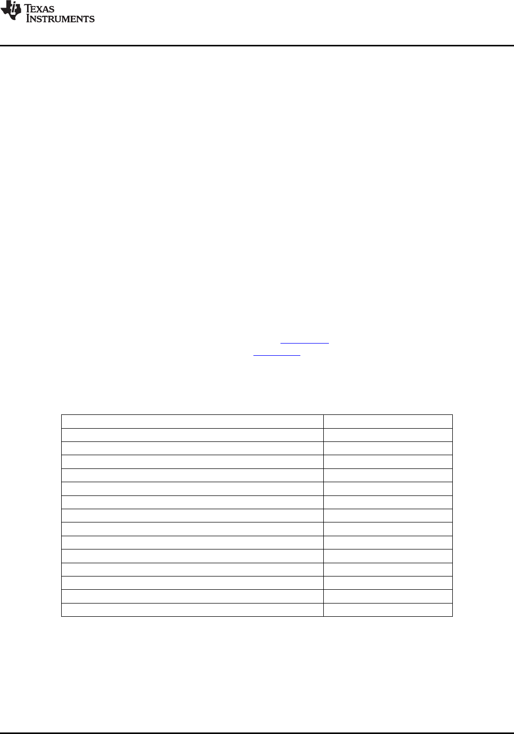
Table 7-60. Default Values for PCI Configuration Registers
REGISTER DEFAULT VALUE (HEX)
0x01C1 A000—Vendor ID/Device ID Register (PCIVENDEV) B002 104Ch
Device ID B002h
Vendor ID 104Ch
0x01C1 A008—Class Code/Revision ID Register (PCICLREV) 1180 0001h
Class Code 80h
Revision ID 01h
0x01C1 A02C—System Vendor ID/Subsystem ID (PCISUBID) 0000 0000h
Subsystem ID 0000
System Vendor ID 0000
0x01C1 A03C—Max Latency/Min Grant/Interrupt Pin/Interrupt Line 0000 0100h
Max Latency 00
Min Grant 00
Interrupt Pin 01
Interrupt Line 00
The on-chip Bootloader supports a host boot which allows an external PCI device to load application code
into the DMSoC's memory space.
Copyright © 2009–2012, Texas Instruments Incorporated Peripheral Information and Electrical Specifications 243
Submit Documentation Feedback
Product Folder Link(s): TMS320DM6467T