
Datasheet


Table Of Contents
- 1 Digital Media System-on-Chip (DMSoC)
- Table of Contents
- 2 Revision History
- 3 Device Overview
- 3.1 Device Characteristics
- 3.2 Device Compatibility
- 3.3 ARM Subsystem
- 3.3.1 ARM926EJ-S RISC CPU
- 3.3.2 CP15
- 3.3.3 MMU
- 3.3.4 Caches and Write Buffer
- 3.3.5 Tightly Coupled Memory (TCM)
- 3.3.6 Advanced High-Performance Bus (AHB)
- 3.3.7 Embedded Trace Macrocell (ETM) and Embedded Trace Buffer (ETB)
- 3.3.8 ARM Memory Mapping
- 3.3.9 Peripherals
- 3.3.10 PLL Controller (PLLC)
- 3.3.11 Power and Sleep Controller (PSC)
- 3.3.12 ARM Interrupt Controller (AINTC)
- 3.3.13 System Module
- 3.3.14 Power Management
- 3.4 DSP Subsystem
- 3.5 Memory Map Summary
- 3.6 Pin Assignments
- 3.7 Terminal Functions
- 3.8 Device Support
- 3.9 Documentation Support
- 3.10 Community Resources
- 4 Device Configurations
- 4.1 System Module Registers
- 4.2 Power Considerations
- 4.3 Clock Considerations
- 4.4 Boot Sequence
- 4.5 Configurations At Reset
- 4.6 Configurations After Reset
- 4.7 Multiplexed Pin Configurations
- 4.7.1 Pin Muxing Selection At Reset
- 4.7.2 Pin Muxing Selection After Reset
- 4.7.3 Pin Multiplexing Details
- 4.7.3.1 PCI, HPI, EMIFA, and ATA Pin Muxing
- 4.7.3.2 PWM Signal Muxing
- 4.7.3.3 TSIF0 Input Signal Muxing (Serial/Parallel)
- 4.7.3.4 TSIF0 Output Signal Muxing (Serial/Parallel)
- 4.7.3.5 TSIF1 Input Signal Muxing (Serial Only)
- 4.7.3.6 TSIF1 Output Signal Muxing (Serial Only)
- 4.7.3.7 CRGEN Signal Muxing
- 4.7.3.8 UART0 Pin Muxing
- 4.7.3.9 UART1 Pin Muxing
- 4.7.3.10 UART2 Pin Muxing
- 4.7.3.11 ARM/DSP Communications Interrupts
- 4.7.3.12 Emulation Control
- 4.8 Debugging Considerations
- 5 System Interconnect
- 6 Device Operating Conditions
- 7 Peripheral Information and Electrical Specifications
- 7.1 Parameter Information
- 7.2 Recommended Clock and Control Signal Transition Behavior
- 7.3 Power Supplies
- 7.4 External Clock Input From DEV_MXI/DEV_CLKIN and AUX_MXI/AUX_CLKIN Pins
- 7.5 Clock PLLs
- 7.6 Enhanced Direct Memory Access (EDMA3) Controller
- 7.7 Reset
- 7.8 Interrupts
- 7.9 External Memory Interface (EMIF)
- 7.10 DDR2 Memory Controller
- 7.10.1 DDR2 Memory Controller Electrical Data/Timing
- 7.10.2 DDR2 Interface
- 7.10.2.1 DDR2 Interface Schematic
- 7.10.2.2 Compatible JEDEC DDR2 Devices
- 7.10.2.3 PCB Stackup
- 7.10.2.4 Placement
- 7.10.2.5 DDR2 Keep Out Region
- 7.10.2.6 Bulk Bypass Capacitors
- 7.10.2.7 High-Speed Bypass Capacitors
- 7.10.2.8 Net Classes
- 7.10.2.9 DDR2 Signal Termination
- 7.10.2.10 VREF Routing
- 7.10.2.11 DDR2 CK and ADDR_CTRL Routing
- 7.11 Video Port Interface (VPIF)
- 7.12 Transport Stream Interface (TSIF)
- 7.13 Clock Recovery Generator (CRGEN)
- 7.14 Video Data Conversion Engine (VDCE)
- 7.15 Peripheral Component Interconnect (PCI)
- 7.16 Ethernet MAC (EMAC)
- 7.17 Management Data Input/Output (MDIO)
- 7.18 Host-Port Interface (HPI) Peripheral
- 7.19 USB 2.0 [see Note]
- 7.20 ATA Controller
- 7.21 VLYNQ
- 7.22 Multichannel Audio Serial Port (McASP0/1) Peripherals
- 7.23 Serial Peripheral Interface (SPI)
- 7.24 Universal Asynchronouse Receiver/Transmitter (UART)
- 7.25 Inter-Integrated Circuit (I2C)
- 7.26 Pulse Width Modulator (PWM)
- 7.27 Timers
- 7.28 General-Purpose Input/Output (GPIO)
- 7.29 IEEE 1149.1 JTAG
- 8 Mechanical Packaging and Orderable Information
TMS320DM6467T
SPRS605C –JULY 2009–REVISED JUNE 2012
www.ti.com
7.14 Video Data Conversion Engine (VDCE)
The DM6467T Video Data Conversion Engine (VDCE) supports the following features:
• Resize function on horizontal (HRSZ) and vertical (VRSZ) with ratio defined by 256/N (N is a natural
number that ranges from 256 to 2048) with 4 taps interpolation. Magnification ratio of horizontal resize
and vertical resize can be configured separately (different value can be configured).
• Anti-alias filter (combination of two kinds of low-pass filter) with horizontal 7 taps, and vertical direction.
• Chrominance signal format conversion (CCV) on both directions, one is from 4:2:2 to 4:2:0 and one is
from 4:2:0 to 4:2:2. This function also uses 4 taps interpolation. MPEG-1 specific format (half-pixel
phased from even pixel position of luminance) is also supported.
• Edge padding for preparation of MC with unrestricted motion vector (required by MPEG-4, H.264, VC-
1). All modes (progressive, interlace frame, and interlace field) are supported (macro-block level
control that is required in H.264 is not currently supported).
• VC-1 range mapping in advanced profile (in case of displaying decoded reference image or trans-
coding from VC-1 to any other format of video codec).
• 2-bit hardware menu overlay with 256 steps of blending for each color.
7.14.1 VDCE Bus Master
The VDCE includes a bus master interface that accesses the DM646x system bus to transfer data.
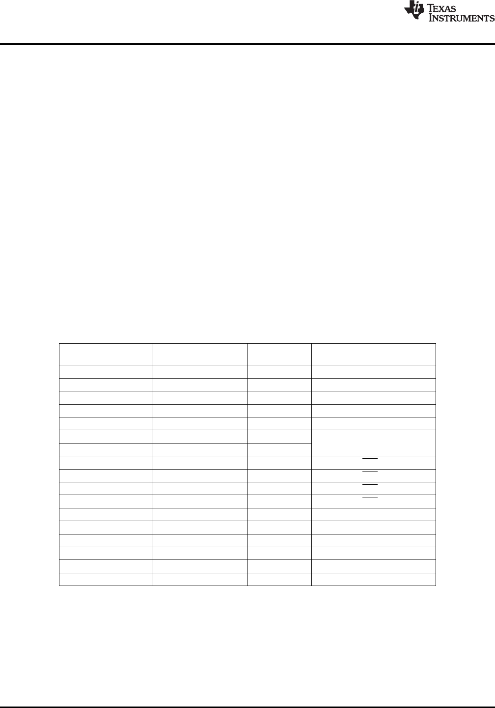
Table 7-58 shows the memory map for the VDCE interface.
Table 7-58. VDCE Master Memory Map
SIZE
START ADDRESS END ADDRESS VDCE ACCESS
(BYTES)
0x0000 0000 0x0FFF FFFF 256M Reserved
0x1000 0000 0x1000 FFFF 64K Reserved
0x1001 0000 0x1001 3FFF 16K ARM RAM 0 (Data)
0x1001 4000 0x1001 7FFF 16K ARM RAM 1 (Data)
0x1001 8000 0x1001 FFFF 32K ARM ROM (Data)
0x1002 0000 0x10FF FFFF 16256K
Reserved
0x1100 0000 0x41FF FFFF 784M
0x4200 0000 0x43FF FFFF 32M EMIFA Data (CS2)
0x4400 0000 0x45FF FFFF 32M EMIFA Data (CS3)
0x4600 0000 0x47FF FFFF 32M EMIFA Data (CS4)
0x4800 0000 0x49FF FFFF 32M EMIFA Data (CS5)
0x4A00 0000 0x4BFF FFFF 32M Reserved
0x4C00 0000 0x4FFF FFFF 64M VLYNQ (Remote Data)
0x5000 0000 0x7FFF FFFF 768M Reserved
0x8000 0000 0x9FFF FFFF 512M DDR2 Memory Controller
0xA000 0000 0xBFFF FFFF 512M Reserved
0xC000 0000 0xFFFF FFFF 1G Reserved
240 Peripheral Information and Electrical Specifications Copyright © 2009–2012, Texas Instruments Incorporated
Submit Documentation Feedback
Product Folder Link(s): TMS320DM6467T