
Datasheet


Table Of Contents
- 1 Digital Media System-on-Chip (DMSoC)
- Table of Contents
- 2 Revision History
- 3 Device Overview
- 3.1 Device Characteristics
- 3.2 Device Compatibility
- 3.3 ARM Subsystem
- 3.3.1 ARM926EJ-S RISC CPU
- 3.3.2 CP15
- 3.3.3 MMU
- 3.3.4 Caches and Write Buffer
- 3.3.5 Tightly Coupled Memory (TCM)
- 3.3.6 Advanced High-Performance Bus (AHB)
- 3.3.7 Embedded Trace Macrocell (ETM) and Embedded Trace Buffer (ETB)
- 3.3.8 ARM Memory Mapping
- 3.3.9 Peripherals
- 3.3.10 PLL Controller (PLLC)
- 3.3.11 Power and Sleep Controller (PSC)
- 3.3.12 ARM Interrupt Controller (AINTC)
- 3.3.13 System Module
- 3.3.14 Power Management
- 3.4 DSP Subsystem
- 3.5 Memory Map Summary
- 3.6 Pin Assignments
- 3.7 Terminal Functions
- 3.8 Device Support
- 3.9 Documentation Support
- 3.10 Community Resources
- 4 Device Configurations
- 4.1 System Module Registers
- 4.2 Power Considerations
- 4.3 Clock Considerations
- 4.4 Boot Sequence
- 4.5 Configurations At Reset
- 4.6 Configurations After Reset
- 4.7 Multiplexed Pin Configurations
- 4.7.1 Pin Muxing Selection At Reset
- 4.7.2 Pin Muxing Selection After Reset
- 4.7.3 Pin Multiplexing Details
- 4.7.3.1 PCI, HPI, EMIFA, and ATA Pin Muxing
- 4.7.3.2 PWM Signal Muxing
- 4.7.3.3 TSIF0 Input Signal Muxing (Serial/Parallel)
- 4.7.3.4 TSIF0 Output Signal Muxing (Serial/Parallel)
- 4.7.3.5 TSIF1 Input Signal Muxing (Serial Only)
- 4.7.3.6 TSIF1 Output Signal Muxing (Serial Only)
- 4.7.3.7 CRGEN Signal Muxing
- 4.7.3.8 UART0 Pin Muxing
- 4.7.3.9 UART1 Pin Muxing
- 4.7.3.10 UART2 Pin Muxing
- 4.7.3.11 ARM/DSP Communications Interrupts
- 4.7.3.12 Emulation Control
- 4.8 Debugging Considerations
- 5 System Interconnect
- 6 Device Operating Conditions
- 7 Peripheral Information and Electrical Specifications
- 7.1 Parameter Information
- 7.2 Recommended Clock and Control Signal Transition Behavior
- 7.3 Power Supplies
- 7.4 External Clock Input From DEV_MXI/DEV_CLKIN and AUX_MXI/AUX_CLKIN Pins
- 7.5 Clock PLLs
- 7.6 Enhanced Direct Memory Access (EDMA3) Controller
- 7.7 Reset
- 7.8 Interrupts
- 7.9 External Memory Interface (EMIF)
- 7.10 DDR2 Memory Controller
- 7.10.1 DDR2 Memory Controller Electrical Data/Timing
- 7.10.2 DDR2 Interface
- 7.10.2.1 DDR2 Interface Schematic
- 7.10.2.2 Compatible JEDEC DDR2 Devices
- 7.10.2.3 PCB Stackup
- 7.10.2.4 Placement
- 7.10.2.5 DDR2 Keep Out Region
- 7.10.2.6 Bulk Bypass Capacitors
- 7.10.2.7 High-Speed Bypass Capacitors
- 7.10.2.8 Net Classes
- 7.10.2.9 DDR2 Signal Termination
- 7.10.2.10 VREF Routing
- 7.10.2.11 DDR2 CK and ADDR_CTRL Routing
- 7.11 Video Port Interface (VPIF)
- 7.12 Transport Stream Interface (TSIF)
- 7.13 Clock Recovery Generator (CRGEN)
- 7.14 Video Data Conversion Engine (VDCE)
- 7.15 Peripheral Component Interconnect (PCI)
- 7.16 Ethernet MAC (EMAC)
- 7.17 Management Data Input/Output (MDIO)
- 7.18 Host-Port Interface (HPI) Peripheral
- 7.19 USB 2.0 [see Note]
- 7.20 ATA Controller
- 7.21 VLYNQ
- 7.22 Multichannel Audio Serial Port (McASP0/1) Peripherals
- 7.23 Serial Peripheral Interface (SPI)
- 7.24 Universal Asynchronouse Receiver/Transmitter (UART)
- 7.25 Inter-Integrated Circuit (I2C)
- 7.26 Pulse Width Modulator (PWM)
- 7.27 Timers
- 7.28 General-Purpose Input/Output (GPIO)
- 7.29 IEEE 1149.1 JTAG
- 8 Mechanical Packaging and Orderable Information
TMS320DM6467T
www.ti.com
SPRS605C –JULY 2009–REVISED JUNE 2012
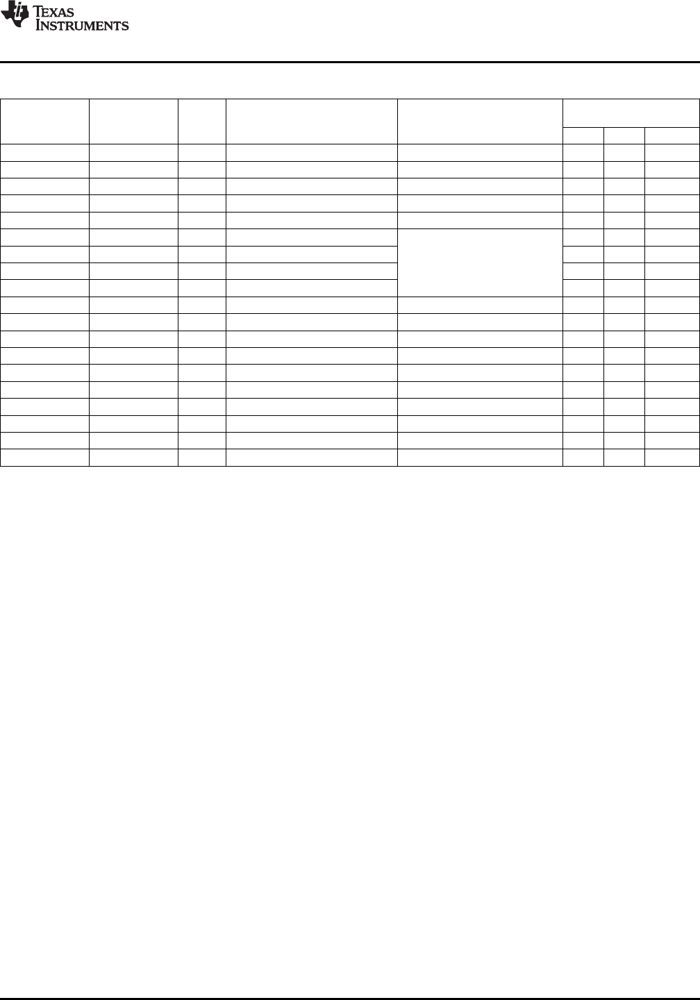
Table 3-4. Configuration Memory Map Summary (continued)
MASTER PERIPHERAL
START END SIZE
ACCESSIBILITY
ARM/EDMA C64x+
ADDRESS ADDRESS (Bytes)
HPI PCI VLYNQ
0x01C6 6000 0x01C6 67FF 2K ATA x x x
0x01C6 6800 0x01C6 6FFF 2K SPI x x x
0x01C6 7000 0x01C6 77FF 2K GPIO x x x
0x01C6 7800 0x01C6 7FFF 2K HPI HPI x x x
0x01C6 8000 0x01C7 FFFF 96K Reserved Reserved x x x
0x01C8 0000 0x01C8 0FFF 4K EMAC Control Registers x x x
0x01C8 1000 0x01C8 1FFF 4K EMAC Control Module Registers x x x
Reserved
0x01C8 2000 0x01C8 3FFF 8K EMAC Control Module RAM x x x
0x01C8 4000 0x01C8 47FF 2K MDIO Control Registers x x x
0x01C8 4800 0x01D0 0FFF 498K Reserved Reserved x x x
0x01D0 1000 0x01D0 13FF 1K McASP0 Registers McASP0 Registers x x x
0x01D0 1400 0x01D0 17FF 1K McASP0 Data Port McASP0 Data Port x x x
0x01D0 1800 0x01D0 1BFF 1K McASP1 Registers McASP1 Registers x x x
0x01D0 1C00 0x01D0 1FFF 1K McASP1 Data Port McASP1 Data Port x x x
0x01D0 2000 0x01DF FFFF 1016K Reserved Reserved
0x01E0 0000 0x01FF FFFF 2M Reserved Reserved
0x0200 0000 0x021F FFFF 2M Reserved Reserved
0x0220 0000 0x023F FFFF 2M Reserved Reserved
0x0240 0000 0x0FFF FFFF 220M Reserved Reserved
3.6 Pin Assignments
Extensive use of pin multiplexing is used to accommodate the largest number of peripheral functions in
the smallest possible package. Pin multiplexing is controlled using a combination of hardware
configuration at device reset and software programmable register settings. For more information on pin
muxing, see Section 4.7, Multiplexed Pin Configurations, of this document.
3.6.1 Pin Map (Bottom View)
Figure 3-2 through Figure 3-7 show the bottom view of the package pin assignments in six quadrants (A,
B, C, D, E, and F).
Copyright © 2009–2012, Texas Instruments Incorporated Device Overview 23
Submit Documentation Feedback
Product Folder Link(s): TMS320DM6467T