
Datasheet


Table Of Contents
- 1 Digital Media System-on-Chip (DMSoC)
- Table of Contents
- 2 Revision History
- 3 Device Overview
- 3.1 Device Characteristics
- 3.2 Device Compatibility
- 3.3 ARM Subsystem
- 3.3.1 ARM926EJ-S RISC CPU
- 3.3.2 CP15
- 3.3.3 MMU
- 3.3.4 Caches and Write Buffer
- 3.3.5 Tightly Coupled Memory (TCM)
- 3.3.6 Advanced High-Performance Bus (AHB)
- 3.3.7 Embedded Trace Macrocell (ETM) and Embedded Trace Buffer (ETB)
- 3.3.8 ARM Memory Mapping
- 3.3.9 Peripherals
- 3.3.10 PLL Controller (PLLC)
- 3.3.11 Power and Sleep Controller (PSC)
- 3.3.12 ARM Interrupt Controller (AINTC)
- 3.3.13 System Module
- 3.3.14 Power Management
- 3.4 DSP Subsystem
- 3.5 Memory Map Summary
- 3.6 Pin Assignments
- 3.7 Terminal Functions
- 3.8 Device Support
- 3.9 Documentation Support
- 3.10 Community Resources
- 4 Device Configurations
- 4.1 System Module Registers
- 4.2 Power Considerations
- 4.3 Clock Considerations
- 4.4 Boot Sequence
- 4.5 Configurations At Reset
- 4.6 Configurations After Reset
- 4.7 Multiplexed Pin Configurations
- 4.7.1 Pin Muxing Selection At Reset
- 4.7.2 Pin Muxing Selection After Reset
- 4.7.3 Pin Multiplexing Details
- 4.7.3.1 PCI, HPI, EMIFA, and ATA Pin Muxing
- 4.7.3.2 PWM Signal Muxing
- 4.7.3.3 TSIF0 Input Signal Muxing (Serial/Parallel)
- 4.7.3.4 TSIF0 Output Signal Muxing (Serial/Parallel)
- 4.7.3.5 TSIF1 Input Signal Muxing (Serial Only)
- 4.7.3.6 TSIF1 Output Signal Muxing (Serial Only)
- 4.7.3.7 CRGEN Signal Muxing
- 4.7.3.8 UART0 Pin Muxing
- 4.7.3.9 UART1 Pin Muxing
- 4.7.3.10 UART2 Pin Muxing
- 4.7.3.11 ARM/DSP Communications Interrupts
- 4.7.3.12 Emulation Control
- 4.8 Debugging Considerations
- 5 System Interconnect
- 6 Device Operating Conditions
- 7 Peripheral Information and Electrical Specifications
- 7.1 Parameter Information
- 7.2 Recommended Clock and Control Signal Transition Behavior
- 7.3 Power Supplies
- 7.4 External Clock Input From DEV_MXI/DEV_CLKIN and AUX_MXI/AUX_CLKIN Pins
- 7.5 Clock PLLs
- 7.6 Enhanced Direct Memory Access (EDMA3) Controller
- 7.7 Reset
- 7.8 Interrupts
- 7.9 External Memory Interface (EMIF)
- 7.10 DDR2 Memory Controller
- 7.10.1 DDR2 Memory Controller Electrical Data/Timing
- 7.10.2 DDR2 Interface
- 7.10.2.1 DDR2 Interface Schematic
- 7.10.2.2 Compatible JEDEC DDR2 Devices
- 7.10.2.3 PCB Stackup
- 7.10.2.4 Placement
- 7.10.2.5 DDR2 Keep Out Region
- 7.10.2.6 Bulk Bypass Capacitors
- 7.10.2.7 High-Speed Bypass Capacitors
- 7.10.2.8 Net Classes
- 7.10.2.9 DDR2 Signal Termination
- 7.10.2.10 VREF Routing
- 7.10.2.11 DDR2 CK and ADDR_CTRL Routing
- 7.11 Video Port Interface (VPIF)
- 7.12 Transport Stream Interface (TSIF)
- 7.13 Clock Recovery Generator (CRGEN)
- 7.14 Video Data Conversion Engine (VDCE)
- 7.15 Peripheral Component Interconnect (PCI)
- 7.16 Ethernet MAC (EMAC)
- 7.17 Management Data Input/Output (MDIO)
- 7.18 Host-Port Interface (HPI) Peripheral
- 7.19 USB 2.0 [see Note]
- 7.20 ATA Controller
- 7.21 VLYNQ
- 7.22 Multichannel Audio Serial Port (McASP0/1) Peripherals
- 7.23 Serial Peripheral Interface (SPI)
- 7.24 Universal Asynchronouse Receiver/Transmitter (UART)
- 7.25 Inter-Integrated Circuit (I2C)
- 7.26 Pulse Width Modulator (PWM)
- 7.27 Timers
- 7.28 General-Purpose Input/Output (GPIO)
- 7.29 IEEE 1149.1 JTAG
- 8 Mechanical Packaging and Orderable Information
TMS320DM6467T
www.ti.com
SPRS605C –JULY 2009–REVISED JUNE 2012
7.12 Transport Stream Interface (TSIF)
The DM6467T device includes two independent Transport Stream Interfaces (TSIF0 and TSIF1) with
corresponding Clock Reference Generator (CRGEN) Modules for System Time-Clock Recovery. The TSIF
peripheral supports the following features:
• 1-bit Serial and 8-bit Parallel independent receive and transmit interfaces with both synchronous and
asynchronous modes. (TSIF1 supports Serial mode only.)
• Stream input/output (I/O) speed rate configurable by the I/O clock speed
• ATS (absolute time stamp) detection, correction, and addition modes
• Automatically detects PAT and PMT and reflects assignment to the internal Packet Identification (PID)
table (supported for partial Transfer Stream [TS] mode only; stream type and PID should be one-to-
one mapping)
• PID filter with 7 PID filter tables and stream type assignments
• BYPASS mode implemented so that not only TS data, but any other data can be received or
transmitted by the TSIF module
• Ring buffer control for both writes (8 channels) and reads (1 channel) to/from memory
• Supports “Specific Packet”, indicating boundary of plural program on TS
• Supports Full-TS in only one mode–Semi-Automatic-A mode, allowing communication to the C64x+
CPU.
• Supports Partial-TS in these modes–Semi-Automatic-B mode and Full-Automatic mode (provided
stream type and PID are one-to-one mapping)
For more detailed information on the CRGEN peripheral, see the TMS320DM646x DMSoC Clock
Reference Generator User's Guide (literature number SPRUEQ1).
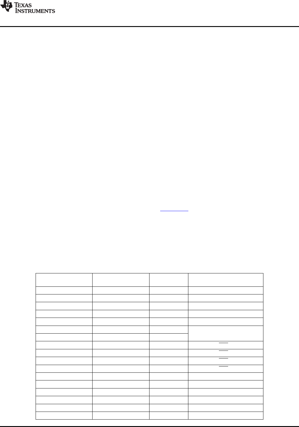
7.12.1 TSIF Bus Master
The TSIF peripherals each include a bus master interface that accesses the DM646x system bus to
transfer stream receive and transmit data. Table 7-49 shows the memory map for the TSIF master
interfaces.
Table 7-49. TSIF0/1 Master Memory Map
SIZE
START ADDRESS END ADDRESS TSIF0/1 ACCESS
(BYTES)
0x0000 0000 0x0FFF FFFF 256M Reserved
0x1000 0000 0x1000 FFFF 64K Reserved
0x1001 0000 0x1001 3FFF 16K ARM RAM 0 (Data)
0x1001 4000 0x1001 7FFF 16K ARM RAM 1 (Data)
0x1001 8000 0x1001 FFFF 32K ARM ROM (Data)
0x1002 0000 0x10FF FFFF 16256K
Reserved
0x1100 0000 0x41FF FFFF 784M
0x4200 0000 0x43FF FFFF 32M EMIFA Data (CS2)
0x4400 0000 0x45FF FFFF 32M EMIFA Data (CS3)
0x4600 0000 0x47FF FFFF 32M EMIFA Data (CS4)
0x4800 0000 0x49FF FFFF 32M EMIFA Data (CS5)
0x4A00 0000 0x4BFF FFFF 32M Reserved
0x4C00 0000 0x4FFF FFFF 64M VLYNQ (Remote Data)
0x5000 0000 0x7FFF FFFF 768M Reserved
0x8000 0000 0x9FFF FFFF 512M DDR2 Memory Controller
0xA000 0000 0xBFFF FFFF 512M Reserved
0xC000 0000 0xFFFF FFFF 1G Reserved
Copyright © 2009–2012, Texas Instruments Incorporated Peripheral Information and Electrical Specifications 227
Submit Documentation Feedback
Product Folder Link(s): TMS320DM6467T