
Datasheet


Table Of Contents
- 1 Digital Media System-on-Chip (DMSoC)
- Table of Contents
- 2 Revision History
- 3 Device Overview
- 3.1 Device Characteristics
- 3.2 Device Compatibility
- 3.3 ARM Subsystem
- 3.3.1 ARM926EJ-S RISC CPU
- 3.3.2 CP15
- 3.3.3 MMU
- 3.3.4 Caches and Write Buffer
- 3.3.5 Tightly Coupled Memory (TCM)
- 3.3.6 Advanced High-Performance Bus (AHB)
- 3.3.7 Embedded Trace Macrocell (ETM) and Embedded Trace Buffer (ETB)
- 3.3.8 ARM Memory Mapping
- 3.3.9 Peripherals
- 3.3.10 PLL Controller (PLLC)
- 3.3.11 Power and Sleep Controller (PSC)
- 3.3.12 ARM Interrupt Controller (AINTC)
- 3.3.13 System Module
- 3.3.14 Power Management
- 3.4 DSP Subsystem
- 3.5 Memory Map Summary
- 3.6 Pin Assignments
- 3.7 Terminal Functions
- 3.8 Device Support
- 3.9 Documentation Support
- 3.10 Community Resources
- 4 Device Configurations
- 4.1 System Module Registers
- 4.2 Power Considerations
- 4.3 Clock Considerations
- 4.4 Boot Sequence
- 4.5 Configurations At Reset
- 4.6 Configurations After Reset
- 4.7 Multiplexed Pin Configurations
- 4.7.1 Pin Muxing Selection At Reset
- 4.7.2 Pin Muxing Selection After Reset
- 4.7.3 Pin Multiplexing Details
- 4.7.3.1 PCI, HPI, EMIFA, and ATA Pin Muxing
- 4.7.3.2 PWM Signal Muxing
- 4.7.3.3 TSIF0 Input Signal Muxing (Serial/Parallel)
- 4.7.3.4 TSIF0 Output Signal Muxing (Serial/Parallel)
- 4.7.3.5 TSIF1 Input Signal Muxing (Serial Only)
- 4.7.3.6 TSIF1 Output Signal Muxing (Serial Only)
- 4.7.3.7 CRGEN Signal Muxing
- 4.7.3.8 UART0 Pin Muxing
- 4.7.3.9 UART1 Pin Muxing
- 4.7.3.10 UART2 Pin Muxing
- 4.7.3.11 ARM/DSP Communications Interrupts
- 4.7.3.12 Emulation Control
- 4.8 Debugging Considerations
- 5 System Interconnect
- 6 Device Operating Conditions
- 7 Peripheral Information and Electrical Specifications
- 7.1 Parameter Information
- 7.2 Recommended Clock and Control Signal Transition Behavior
- 7.3 Power Supplies
- 7.4 External Clock Input From DEV_MXI/DEV_CLKIN and AUX_MXI/AUX_CLKIN Pins
- 7.5 Clock PLLs
- 7.6 Enhanced Direct Memory Access (EDMA3) Controller
- 7.7 Reset
- 7.8 Interrupts
- 7.9 External Memory Interface (EMIF)
- 7.10 DDR2 Memory Controller
- 7.10.1 DDR2 Memory Controller Electrical Data/Timing
- 7.10.2 DDR2 Interface
- 7.10.2.1 DDR2 Interface Schematic
- 7.10.2.2 Compatible JEDEC DDR2 Devices
- 7.10.2.3 PCB Stackup
- 7.10.2.4 Placement
- 7.10.2.5 DDR2 Keep Out Region
- 7.10.2.6 Bulk Bypass Capacitors
- 7.10.2.7 High-Speed Bypass Capacitors
- 7.10.2.8 Net Classes
- 7.10.2.9 DDR2 Signal Termination
- 7.10.2.10 VREF Routing
- 7.10.2.11 DDR2 CK and ADDR_CTRL Routing
- 7.11 Video Port Interface (VPIF)
- 7.12 Transport Stream Interface (TSIF)
- 7.13 Clock Recovery Generator (CRGEN)
- 7.14 Video Data Conversion Engine (VDCE)
- 7.15 Peripheral Component Interconnect (PCI)
- 7.16 Ethernet MAC (EMAC)
- 7.17 Management Data Input/Output (MDIO)
- 7.18 Host-Port Interface (HPI) Peripheral
- 7.19 USB 2.0 [see Note]
- 7.20 ATA Controller
- 7.21 VLYNQ
- 7.22 Multichannel Audio Serial Port (McASP0/1) Peripherals
- 7.23 Serial Peripheral Interface (SPI)
- 7.24 Universal Asynchronouse Receiver/Transmitter (UART)
- 7.25 Inter-Integrated Circuit (I2C)
- 7.26 Pulse Width Modulator (PWM)
- 7.27 Timers
- 7.28 General-Purpose Input/Output (GPIO)
- 7.29 IEEE 1149.1 JTAG
- 8 Mechanical Packaging and Orderable Information
VP_CLKIN0
VPIF
Channel0
InputClockSource
VP_CLKIN0
VSCLKDIS.VID0
TMS320DM6467T
www.ti.com
SPRS605C –JULY 2009–REVISED JUNE 2012
7.11 Video Port Interface (VPIF)
The DM6467T Video Port Interface (VPIF) allows the capture and display of digital video streams.
Features include:
• 150-MHz VPIF
• Up to 2 Video Capture Channels (Channel 0 and Channel 1)
– Two 8-bit Standard-Definition (SD) Video with embedded timing codes (BT.656)
– Single 16-bit High-Definition (HD) Video with embedded timing codes (BT.1120)
– Single Raw Video (8-/10-/12-bit)
• Up to 2 Video Display Channels (Channel 2 and Channel 3)
– Two 8-bit SD Video Display with embedded timing codes (BT.656)
– Single 16-bit HD Video Display with embedded timing codes (BT.1120)
The VPIF capture channel input data format is selectable based on the settings of the specific Channel
Control Register (Channels 0–3). The VPIF Raw Video data-bus width is selectable based on the settings
of the Channel 0 Control Register. For more detailed information on these specific Channel Control
Registers, see the TMS320DM6467x DMSoC Video Port Interface (VPIF) User's Guide (Literature
Number SPRUER9).
7.11.1 VPIF Bus Master Memory Map
The VPIF peripheral includes a bus master interface that accesses the DM6467T system bus to transfer
video-capture and video-display data. Table 7-44 shows the memory map for the VPIF master interface.
Table 7-44. VPIF Master Memory Map
START END SIZE
VPIF MASTER INTERFACE
ADDRESS ADDRESS (BYTES)
0x0000 0000 0x7FFF FFFF 2G Reserved
0x8000 0000 0x9FFF FFFF 512M DDR2 Memory Controller
0xA000 0000 0xBFFF FFFF 512M Reserved
0xC000 0000 0xFFFF FFFF 1G Reserved
7.11.2 VPIF Clock Control (Capture and Display)
The source clocks for the VPIF data channels are selectable based on the settings of the VIDCLKCTL
register (0x01C4 0038) (For the VIDCLKCTL register details, see Section 4.3.2.1, Video Clock Control
Register). The VSCLKDIS register (0x01C4 006C) is used to disable the clock inputs when changing the
clock source to ensure glitch-free operation. (For the VSCLKDIS register details, see Section 4.3.2.3,
Video and TSIF Clock Disable).
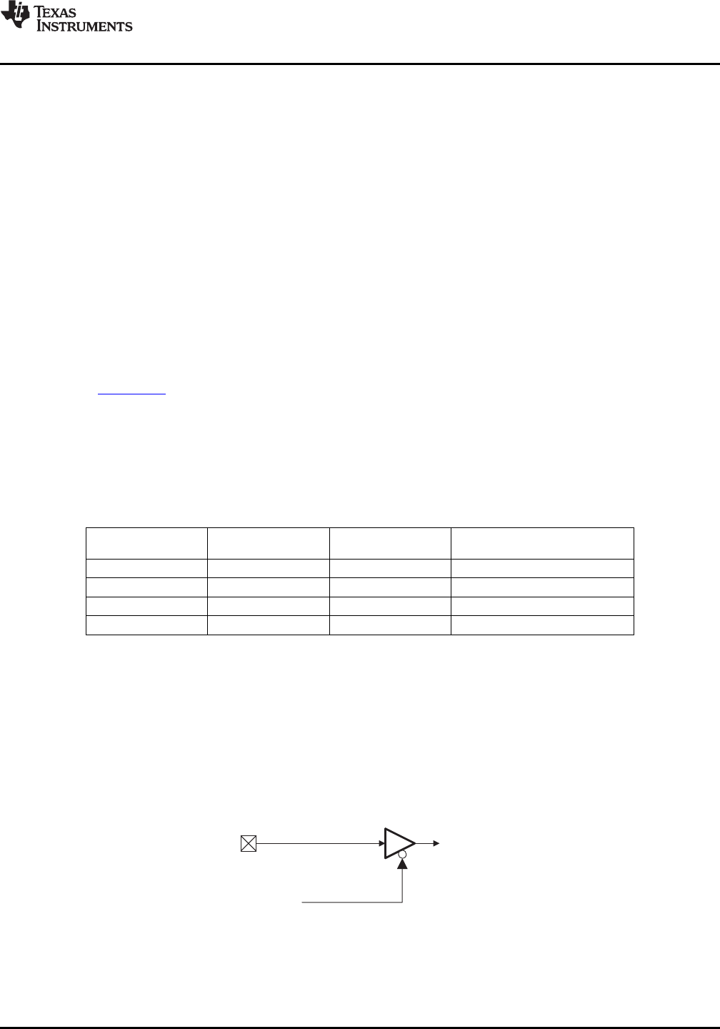
For both the VPIF dual 8-bit or 16-bit video-capture modes, Channel 0 is always clocked by VP_CLKIN0
(see Figure 7-34).
Figure 7-34. VPIF Capture Channel 0 Source Clock
Video-Capture Channel 1 is clocked by the VP_CLKIN1 signal, when the dual 8-bit capture mode is
enabled. When the 16-bit capture mode or 8-/10-/12-bit raw-capture mode is used, VP_CLKIN0 must be
selected as the clock source (VIDCLKCTL.VCH1CLK = 0) [see Figure 7-35].
Copyright © 2009–2012, Texas Instruments Incorporated Peripheral Information and Electrical Specifications 219
Submit Documentation Feedback
Product Folder Link(s): TMS320DM6467T