
Datasheet


Table Of Contents
- 1 Digital Media System-on-Chip (DMSoC)
- Table of Contents
- 2 Revision History
- 3 Device Overview
- 3.1 Device Characteristics
- 3.2 Device Compatibility
- 3.3 ARM Subsystem
- 3.3.1 ARM926EJ-S RISC CPU
- 3.3.2 CP15
- 3.3.3 MMU
- 3.3.4 Caches and Write Buffer
- 3.3.5 Tightly Coupled Memory (TCM)
- 3.3.6 Advanced High-Performance Bus (AHB)
- 3.3.7 Embedded Trace Macrocell (ETM) and Embedded Trace Buffer (ETB)
- 3.3.8 ARM Memory Mapping
- 3.3.9 Peripherals
- 3.3.10 PLL Controller (PLLC)
- 3.3.11 Power and Sleep Controller (PSC)
- 3.3.12 ARM Interrupt Controller (AINTC)
- 3.3.13 System Module
- 3.3.14 Power Management
- 3.4 DSP Subsystem
- 3.5 Memory Map Summary
- 3.6 Pin Assignments
- 3.7 Terminal Functions
- 3.8 Device Support
- 3.9 Documentation Support
- 3.10 Community Resources
- 4 Device Configurations
- 4.1 System Module Registers
- 4.2 Power Considerations
- 4.3 Clock Considerations
- 4.4 Boot Sequence
- 4.5 Configurations At Reset
- 4.6 Configurations After Reset
- 4.7 Multiplexed Pin Configurations
- 4.7.1 Pin Muxing Selection At Reset
- 4.7.2 Pin Muxing Selection After Reset
- 4.7.3 Pin Multiplexing Details
- 4.7.3.1 PCI, HPI, EMIFA, and ATA Pin Muxing
- 4.7.3.2 PWM Signal Muxing
- 4.7.3.3 TSIF0 Input Signal Muxing (Serial/Parallel)
- 4.7.3.4 TSIF0 Output Signal Muxing (Serial/Parallel)
- 4.7.3.5 TSIF1 Input Signal Muxing (Serial Only)
- 4.7.3.6 TSIF1 Output Signal Muxing (Serial Only)
- 4.7.3.7 CRGEN Signal Muxing
- 4.7.3.8 UART0 Pin Muxing
- 4.7.3.9 UART1 Pin Muxing
- 4.7.3.10 UART2 Pin Muxing
- 4.7.3.11 ARM/DSP Communications Interrupts
- 4.7.3.12 Emulation Control
- 4.8 Debugging Considerations
- 5 System Interconnect
- 6 Device Operating Conditions
- 7 Peripheral Information and Electrical Specifications
- 7.1 Parameter Information
- 7.2 Recommended Clock and Control Signal Transition Behavior
- 7.3 Power Supplies
- 7.4 External Clock Input From DEV_MXI/DEV_CLKIN and AUX_MXI/AUX_CLKIN Pins
- 7.5 Clock PLLs
- 7.6 Enhanced Direct Memory Access (EDMA3) Controller
- 7.7 Reset
- 7.8 Interrupts
- 7.9 External Memory Interface (EMIF)
- 7.10 DDR2 Memory Controller
- 7.10.1 DDR2 Memory Controller Electrical Data/Timing
- 7.10.2 DDR2 Interface
- 7.10.2.1 DDR2 Interface Schematic
- 7.10.2.2 Compatible JEDEC DDR2 Devices
- 7.10.2.3 PCB Stackup
- 7.10.2.4 Placement
- 7.10.2.5 DDR2 Keep Out Region
- 7.10.2.6 Bulk Bypass Capacitors
- 7.10.2.7 High-Speed Bypass Capacitors
- 7.10.2.8 Net Classes
- 7.10.2.9 DDR2 Signal Termination
- 7.10.2.10 VREF Routing
- 7.10.2.11 DDR2 CK and ADDR_CTRL Routing
- 7.11 Video Port Interface (VPIF)
- 7.12 Transport Stream Interface (TSIF)
- 7.13 Clock Recovery Generator (CRGEN)
- 7.14 Video Data Conversion Engine (VDCE)
- 7.15 Peripheral Component Interconnect (PCI)
- 7.16 Ethernet MAC (EMAC)
- 7.17 Management Data Input/Output (MDIO)
- 7.18 Host-Port Interface (HPI) Peripheral
- 7.19 USB 2.0 [see Note]
- 7.20 ATA Controller
- 7.21 VLYNQ
- 7.22 Multichannel Audio Serial Port (McASP0/1) Peripherals
- 7.23 Serial Peripheral Interface (SPI)
- 7.24 Universal Asynchronouse Receiver/Transmitter (UART)
- 7.25 Inter-Integrated Circuit (I2C)
- 7.26 Pulse Width Modulator (PWM)
- 7.27 Timers
- 7.28 General-Purpose Input/Output (GPIO)
- 7.29 IEEE 1149.1 JTAG
- 8 Mechanical Packaging and Orderable Information
A1
A1
X
Y
OFFSET
RecommendedDDR2Device
Orientation
Y
Y
OFFSET
DDR2
Device
DDR2
Controller
DM646x
TMS320DM6467T
www.ti.com
SPRS605C –JULY 2009–REVISED JUNE 2012
Table 7-34. PCB Stack Up Specifications (continued)
No. Parameter Min Typ Max Unit
2 Signal Routing Layers 3
3 Full ground layers under DDR2 routing Region 2
4 Number of ground plane cuts allowed within DDR routing region 0
5 Number of ground reference planes required for each DDR2 routing layer 1
6 Number of layers between DDR2 routing layer and reference ground plane 0
7 PCB Routing Feature Size 4 Mils
8 PCB Trace Width w 4 Mils
8 PCB BGA escape via pad size 18 Mils
9 PCB BGA escape via hole size 8 Mils
10 DSP Device BGA pad size
(1)
11 DDR2 Device BGA pad size
(2)
12 Single Ended Impedance, Zo 50 75 Ω
13 Impedance Control
(3)
Z-5 Z Z+5 Ω
(1) See the Flip Chip Ball Grid Array Package Reference Guide (SPRU811) for DSP device BGA pad size.
(2) See the DDR2 device manufacturer documenation for the DDR2 device BGA pad size.
(3) Z is the nominal singled ended impedance selected for the PCB specified by item 12.
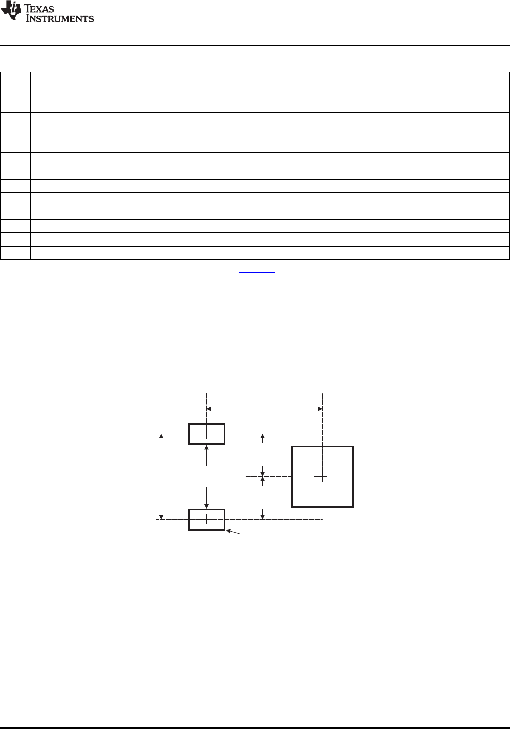
7.10.2.4 Placement
Figure 7-28 shows the required placement for the DM6467T device as well as the DDR2 devices. The
dimensions for Figure 7-28 are defined in Table 7-35. The placement does not restrict the side of the PCB
that the devices are mounted on. The ultimate purpose of the placement is to limit the maximum trace
lengths and allow for proper routing space. For a 16 bit DDR memory systems, the high word DDR2
device is omitted from the placement.
Figure 7-28. DM6467T and DDR2 Device Placement
Copyright © 2009–2012, Texas Instruments Incorporated Peripheral Information and Electrical Specifications 211
Submit Documentation Feedback
Product Folder Link(s): TMS320DM6467T