
Datasheet


Table Of Contents
- 1 Digital Media System-on-Chip (DMSoC)
- Table of Contents
- 2 Revision History
- 3 Device Overview
- 3.1 Device Characteristics
- 3.2 Device Compatibility
- 3.3 ARM Subsystem
- 3.3.1 ARM926EJ-S RISC CPU
- 3.3.2 CP15
- 3.3.3 MMU
- 3.3.4 Caches and Write Buffer
- 3.3.5 Tightly Coupled Memory (TCM)
- 3.3.6 Advanced High-Performance Bus (AHB)
- 3.3.7 Embedded Trace Macrocell (ETM) and Embedded Trace Buffer (ETB)
- 3.3.8 ARM Memory Mapping
- 3.3.9 Peripherals
- 3.3.10 PLL Controller (PLLC)
- 3.3.11 Power and Sleep Controller (PSC)
- 3.3.12 ARM Interrupt Controller (AINTC)
- 3.3.13 System Module
- 3.3.14 Power Management
- 3.4 DSP Subsystem
- 3.5 Memory Map Summary
- 3.6 Pin Assignments
- 3.7 Terminal Functions
- 3.8 Device Support
- 3.9 Documentation Support
- 3.10 Community Resources
- 4 Device Configurations
- 4.1 System Module Registers
- 4.2 Power Considerations
- 4.3 Clock Considerations
- 4.4 Boot Sequence
- 4.5 Configurations At Reset
- 4.6 Configurations After Reset
- 4.7 Multiplexed Pin Configurations
- 4.7.1 Pin Muxing Selection At Reset
- 4.7.2 Pin Muxing Selection After Reset
- 4.7.3 Pin Multiplexing Details
- 4.7.3.1 PCI, HPI, EMIFA, and ATA Pin Muxing
- 4.7.3.2 PWM Signal Muxing
- 4.7.3.3 TSIF0 Input Signal Muxing (Serial/Parallel)
- 4.7.3.4 TSIF0 Output Signal Muxing (Serial/Parallel)
- 4.7.3.5 TSIF1 Input Signal Muxing (Serial Only)
- 4.7.3.6 TSIF1 Output Signal Muxing (Serial Only)
- 4.7.3.7 CRGEN Signal Muxing
- 4.7.3.8 UART0 Pin Muxing
- 4.7.3.9 UART1 Pin Muxing
- 4.7.3.10 UART2 Pin Muxing
- 4.7.3.11 ARM/DSP Communications Interrupts
- 4.7.3.12 Emulation Control
- 4.8 Debugging Considerations
- 5 System Interconnect
- 6 Device Operating Conditions
- 7 Peripheral Information and Electrical Specifications
- 7.1 Parameter Information
- 7.2 Recommended Clock and Control Signal Transition Behavior
- 7.3 Power Supplies
- 7.4 External Clock Input From DEV_MXI/DEV_CLKIN and AUX_MXI/AUX_CLKIN Pins
- 7.5 Clock PLLs
- 7.6 Enhanced Direct Memory Access (EDMA3) Controller
- 7.7 Reset
- 7.8 Interrupts
- 7.9 External Memory Interface (EMIF)
- 7.10 DDR2 Memory Controller
- 7.10.1 DDR2 Memory Controller Electrical Data/Timing
- 7.10.2 DDR2 Interface
- 7.10.2.1 DDR2 Interface Schematic
- 7.10.2.2 Compatible JEDEC DDR2 Devices
- 7.10.2.3 PCB Stackup
- 7.10.2.4 Placement
- 7.10.2.5 DDR2 Keep Out Region
- 7.10.2.6 Bulk Bypass Capacitors
- 7.10.2.7 High-Speed Bypass Capacitors
- 7.10.2.8 Net Classes
- 7.10.2.9 DDR2 Signal Termination
- 7.10.2.10 VREF Routing
- 7.10.2.11 DDR2 CK and ADDR_CTRL Routing
- 7.11 Video Port Interface (VPIF)
- 7.12 Transport Stream Interface (TSIF)
- 7.13 Clock Recovery Generator (CRGEN)
- 7.14 Video Data Conversion Engine (VDCE)
- 7.15 Peripheral Component Interconnect (PCI)
- 7.16 Ethernet MAC (EMAC)
- 7.17 Management Data Input/Output (MDIO)
- 7.18 Host-Port Interface (HPI) Peripheral
- 7.19 USB 2.0 [see Note]
- 7.20 ATA Controller
- 7.21 VLYNQ
- 7.22 Multichannel Audio Serial Port (McASP0/1) Peripherals
- 7.23 Serial Peripheral Interface (SPI)
- 7.24 Universal Asynchronouse Receiver/Transmitter (UART)
- 7.25 Inter-Integrated Circuit (I2C)
- 7.26 Pulse Width Modulator (PWM)
- 7.27 Timers
- 7.28 General-Purpose Input/Output (GPIO)
- 7.29 IEEE 1149.1 JTAG
- 8 Mechanical Packaging and Orderable Information
DDR_CLK
1
TMS320DM6467T
www.ti.com
SPRS605C –JULY 2009–REVISED JUNE 2012
7.10.1 DDR2 Memory Controller Electrical Data/Timing
TI only supports board designs that follow the guidelines outlined in this document.
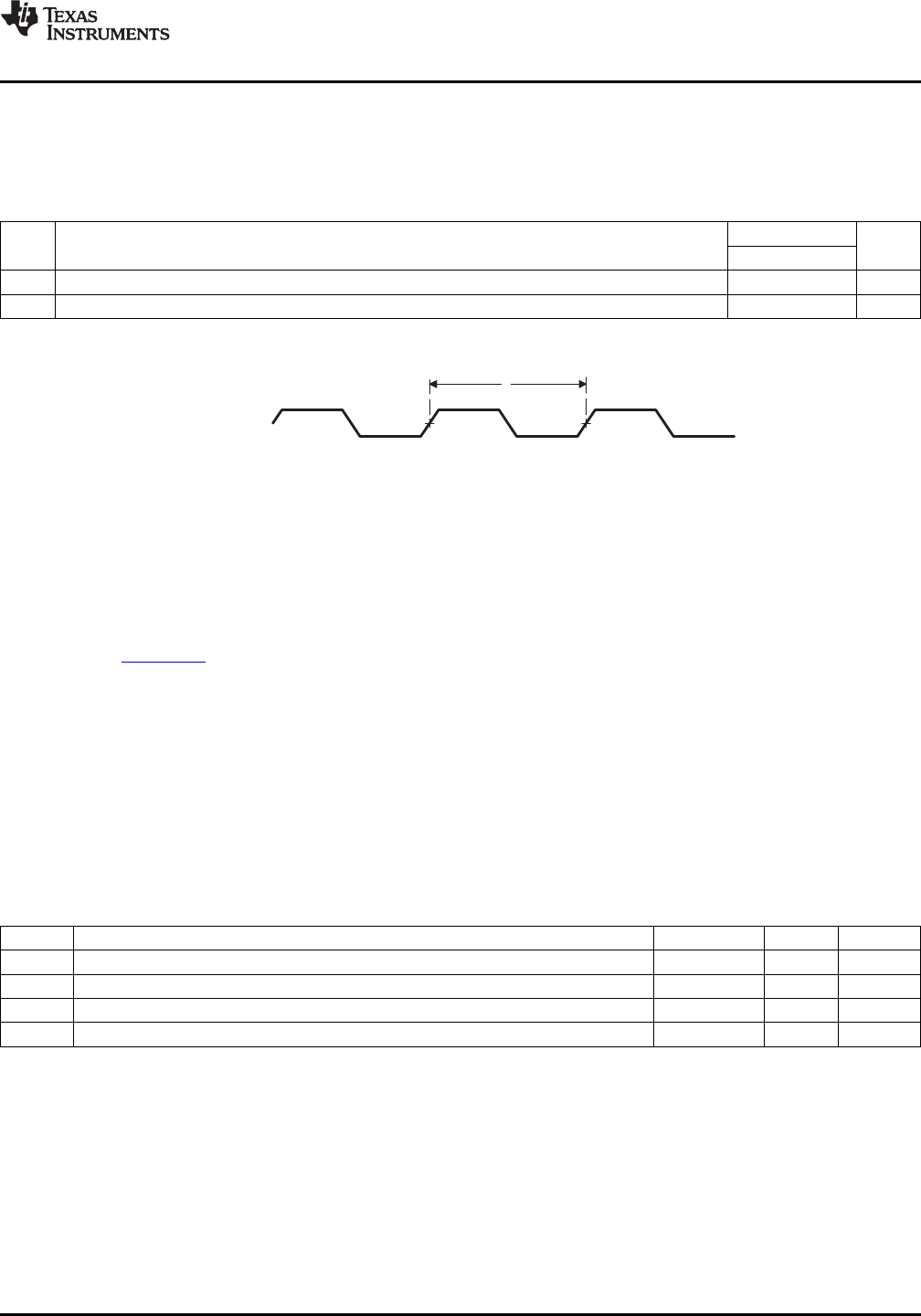
Table 7-31. Switching Characteristics Over Recommended Operating Conditions for DDR2 Memory
Controller
(1) (2)
(see Figure 7-25)
-1G
NO. PARAMETER UNIT
MIN MAX
1 t
c(DDR_CLK)
Cycle time, DDR_CLK 2.5 8 ns
2 f
(DDR_CLK)
Frequency, DDR_CLK 125 400 MHz
(1) DDR_CLK cycle time = 2 x PLL2 _SYSCLK1 cycle time.
(2) The PLL2 Controller must be programmed such that the resulting DDR_CLK clock frequency is within the specified range.
Figure 7-25. DDR2 Memory Controller Clock Timing
7.10.2 DDR2 Interface
This section provides the timing specification for the DDR2 interface as a PCB design and manufacturing
specification. The design rules constrain PCB trace length, PCB trace skew, signal integrity, cross-talk,
and signal timing. These rules, when followed, result in a reliable DDR2 memory system without the need
for a complex timing closure process. For more information regarding the guidelines for using this DDR2
specification, see Understanding TI’s PCB Routing Rule-Based DDR2 Timing Specification Application
Report (SPRAAV0).
7.10.2.1 DDR2 Interface Schematic
Figure 7-26 shows the DDR2 interface schematic for a x32 DDR2 memory system. The x16 DDR2 system
schematic is identical except that the high word DDR2 device is deleted, see Figure 7-27. The pin
numbers for the DM6467T can be obtained from the Section 3.6, Pin Assignments of this document.
7.10.2.2 Compatible JEDEC DDR2 Devices
Table 7-32 shows the parameters of the JEDEC DDR2 devices that are compatible with this interface.
Generally, the DDR2 interface is compatible with x16 DDR2-800 speed grade DDR2 devices.
Table 7-32. Compatible JEDEC DDR2 Devices
No. Parameter Min Max Unit
1 JEDEC DDR2 Device Speed Grade
(1)
DDR2-800
2 JEDEC DDR2 Device Bit Width x16 x16 Bits
3 JEDEC DDR2 Device Count
(2)
1 2 Devices
4 JEDEC DDR2 Device Ball Count
(3)
84 92 Balls
(1) Higher DDR2 speed grades are supported due to inherent JEDEC DDR2 backwards compatibility.
(2) 1 DDR2 device is used for 16 bit DDR2 memory system. 2 DDR2 devices are used for 32 bit DDR2 memory system.
(3) 92 ball devices retained for legacy support. New designs will migrate to 84 ball DDR2 devices. Electrrically the 92 and 84 ball DDR2
devices are the same.
Copyright © 2009–2012, Texas Instruments Incorporated Peripheral Information and Electrical Specifications 207
Submit Documentation Feedback
Product Folder Link(s): TMS320DM6467T