
Datasheet


Table Of Contents
- 1 Digital Media System-on-Chip (DMSoC)
- Table of Contents
- 2 Revision History
- 3 Device Overview
- 3.1 Device Characteristics
- 3.2 Device Compatibility
- 3.3 ARM Subsystem
- 3.3.1 ARM926EJ-S RISC CPU
- 3.3.2 CP15
- 3.3.3 MMU
- 3.3.4 Caches and Write Buffer
- 3.3.5 Tightly Coupled Memory (TCM)
- 3.3.6 Advanced High-Performance Bus (AHB)
- 3.3.7 Embedded Trace Macrocell (ETM) and Embedded Trace Buffer (ETB)
- 3.3.8 ARM Memory Mapping
- 3.3.9 Peripherals
- 3.3.10 PLL Controller (PLLC)
- 3.3.11 Power and Sleep Controller (PSC)
- 3.3.12 ARM Interrupt Controller (AINTC)
- 3.3.13 System Module
- 3.3.14 Power Management
- 3.4 DSP Subsystem
- 3.5 Memory Map Summary
- 3.6 Pin Assignments
- 3.7 Terminal Functions
- 3.8 Device Support
- 3.9 Documentation Support
- 3.10 Community Resources
- 4 Device Configurations
- 4.1 System Module Registers
- 4.2 Power Considerations
- 4.3 Clock Considerations
- 4.4 Boot Sequence
- 4.5 Configurations At Reset
- 4.6 Configurations After Reset
- 4.7 Multiplexed Pin Configurations
- 4.7.1 Pin Muxing Selection At Reset
- 4.7.2 Pin Muxing Selection After Reset
- 4.7.3 Pin Multiplexing Details
- 4.7.3.1 PCI, HPI, EMIFA, and ATA Pin Muxing
- 4.7.3.2 PWM Signal Muxing
- 4.7.3.3 TSIF0 Input Signal Muxing (Serial/Parallel)
- 4.7.3.4 TSIF0 Output Signal Muxing (Serial/Parallel)
- 4.7.3.5 TSIF1 Input Signal Muxing (Serial Only)
- 4.7.3.6 TSIF1 Output Signal Muxing (Serial Only)
- 4.7.3.7 CRGEN Signal Muxing
- 4.7.3.8 UART0 Pin Muxing
- 4.7.3.9 UART1 Pin Muxing
- 4.7.3.10 UART2 Pin Muxing
- 4.7.3.11 ARM/DSP Communications Interrupts
- 4.7.3.12 Emulation Control
- 4.8 Debugging Considerations
- 5 System Interconnect
- 6 Device Operating Conditions
- 7 Peripheral Information and Electrical Specifications
- 7.1 Parameter Information
- 7.2 Recommended Clock and Control Signal Transition Behavior
- 7.3 Power Supplies
- 7.4 External Clock Input From DEV_MXI/DEV_CLKIN and AUX_MXI/AUX_CLKIN Pins
- 7.5 Clock PLLs
- 7.6 Enhanced Direct Memory Access (EDMA3) Controller
- 7.7 Reset
- 7.8 Interrupts
- 7.9 External Memory Interface (EMIF)
- 7.10 DDR2 Memory Controller
- 7.10.1 DDR2 Memory Controller Electrical Data/Timing
- 7.10.2 DDR2 Interface
- 7.10.2.1 DDR2 Interface Schematic
- 7.10.2.2 Compatible JEDEC DDR2 Devices
- 7.10.2.3 PCB Stackup
- 7.10.2.4 Placement
- 7.10.2.5 DDR2 Keep Out Region
- 7.10.2.6 Bulk Bypass Capacitors
- 7.10.2.7 High-Speed Bypass Capacitors
- 7.10.2.8 Net Classes
- 7.10.2.9 DDR2 Signal Termination
- 7.10.2.10 VREF Routing
- 7.10.2.11 DDR2 CK and ADDR_CTRL Routing
- 7.11 Video Port Interface (VPIF)
- 7.12 Transport Stream Interface (TSIF)
- 7.13 Clock Recovery Generator (CRGEN)
- 7.14 Video Data Conversion Engine (VDCE)
- 7.15 Peripheral Component Interconnect (PCI)
- 7.16 Ethernet MAC (EMAC)
- 7.17 Management Data Input/Output (MDIO)
- 7.18 Host-Port Interface (HPI) Peripheral
- 7.19 USB 2.0 [see Note]
- 7.20 ATA Controller
- 7.21 VLYNQ
- 7.22 Multichannel Audio Serial Port (McASP0/1) Peripherals
- 7.23 Serial Peripheral Interface (SPI)
- 7.24 Universal Asynchronouse Receiver/Transmitter (UART)
- 7.25 Inter-Integrated Circuit (I2C)
- 7.26 Pulse Width Modulator (PWM)
- 7.27 Timers
- 7.28 General-Purpose Input/Output (GPIO)
- 7.29 IEEE 1149.1 JTAG
- 8 Mechanical Packaging and Orderable Information
TMS320DM6467T
SPRS605C –JULY 2009–REVISED JUNE 2012
www.ti.com
7.8.2 DSP Interrupts
The C64x+ DSP interrupt controller combines device events into 12 prioritized interrupts. The source for
each of the 12 CPU interrupts is user-programmable and is listed in Table 7-25. Also, the interrupt
controller controls the generation of the CPU exception, NMI, and emulation interrupts. Table 7-26
summarizes the C64x+ interrupt controller registers and memory locations. For more details on DSP
interrupt control, see the TMS320DM646x DMSoC DSP Subsystem Reference Guide (literature number
SPRUEP8).
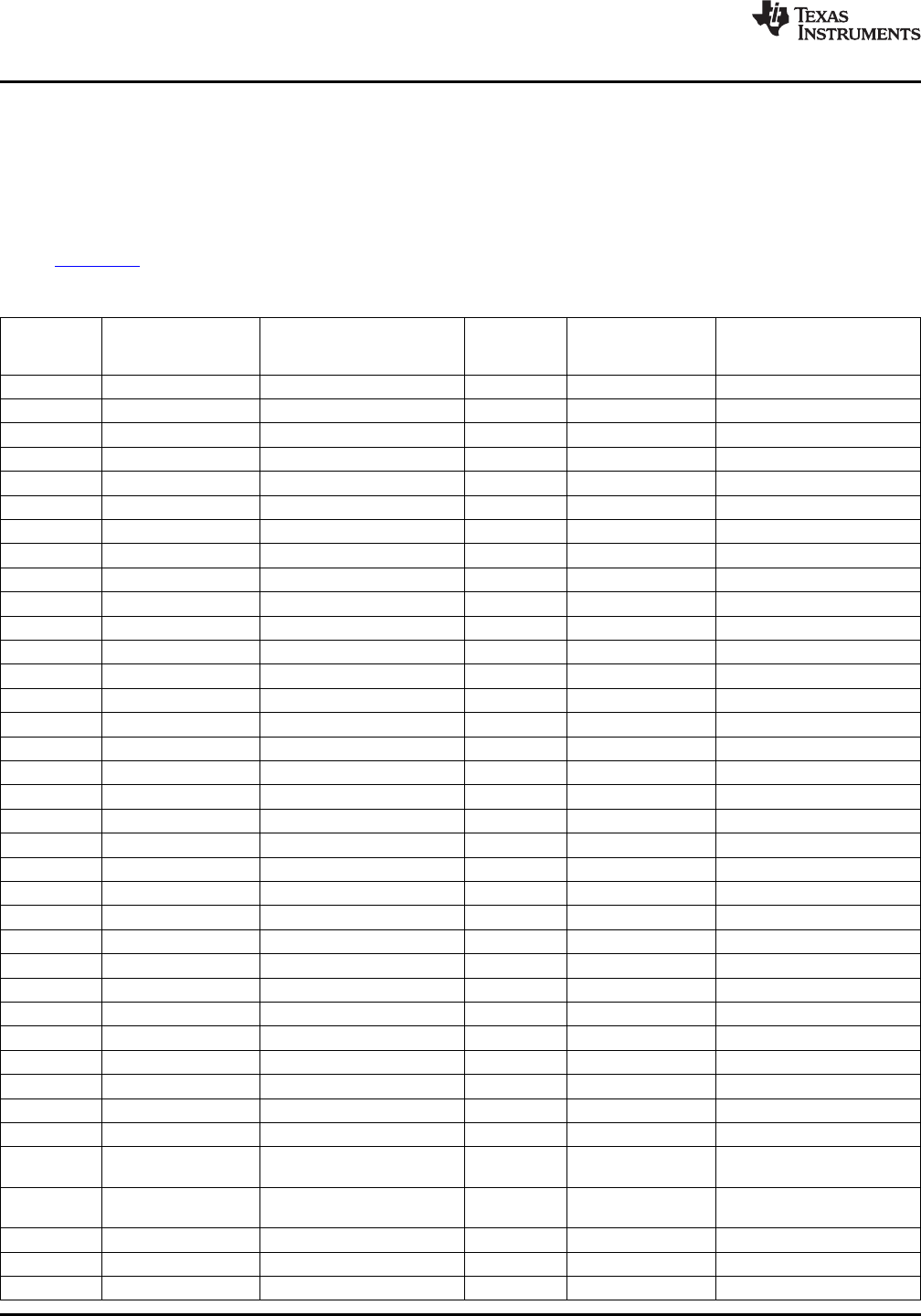
Table 7-25. DM6467T DSP Interrupts
DSP DSP
INTERRUPT ACRONYM SOURCE INTERRUPT ACRONYM SOURCE
NUMBER NUMBER
0 EVT0 C64x+ Int Ctl 0 64 GPIO0 GPIO
1 EVT1 C64x+ Int Ctl 1 65 GPIO1 GPIO
2 EVT2 C64x+ Int Ctl 2 66 GPIO2 GPIO
3 EVT3 C64x+ Int Ctl 3 67 GPIO3 GPIO
4 TINTL0 Timer 0 lower – TINT12 68 GPIO4 GPIO
5 TINTH0 Timer 0 upper – TINT34 69 GPIO5 GPIO
6 TINTL1 Timer 1 lower – TINT12 70 GPIO6 GPIO
7 TINTH1 Timer 1 upper – TINT34 71 GPIO7 GPIO
8 – Reserved 72 – Reserved
9 EMU_DTDMA C64x+ EMC 73 – Reserved
10 – Reserved 74 – Reserved
11 EMU_RTDXRX C64x+ RTDX 75 – Reserved
12 EMU_RTDXTX C64x+ RTDX 76 – Reserved
13 IDMAINT0 C64x+ EMC 0 77 – Reserved
14 IDMAINT1 C64x+ EMC 1 78 – Reserved
15 – Reserved 79 – Reserved
16 ARM2DSP0 ARM to DSP Controller 0 80 – Reserved
17 ARM2DSP1 ARM to DSP Controller 1 81 – Reserved
18 ARM2DSP2 ARM to DSP Controller 2 82 – Reserved
19 ARM2DSP3 ARM to DSP Controller 3 83 – Reserved
20 – Reserved 84 CCINT1 EDMA CC Region 1
21 – Reserved 85 CCERRINT EDMA CC Error
22 – Reserved 86 TCERRINT0 EDMA TC0 Error
23 – Reserved 87 TCERRINT1 EDMA TC1 Error
24 – Reserved 88 TCERRINT2 EDMA TC2 Error
25 – Reserved 89 TCERRINT3 EDMA TC3 Error
26 – Reserved 90 IDEINT ATA
27 – Reserved 91 – Reserved
28 – Reserved 92 – Reserved
29 – Reserved 93 – Reserved
30 – Reserved 94 – Reserved
31 – Reserved 95 – Reserved
– Reserved INTERR C64x+ Interrupt Controller
32 96
Dropped CPU Interrupt Event
– Reserved EMC_IDMAERR C64x+ EMC Invalid IDMA
33 97
Parameters
34 – Reserved 98 – Reserved
35 – Reserved 99 – Reserved
36 – Reserved 100 – Reserved
196 Peripheral Information and Electrical Specifications Copyright © 2009–2012, Texas Instruments Incorporated
Submit Documentation Feedback
Product Folder Link(s): TMS320DM6467T