
Datasheet


Table Of Contents
- 1 Digital Media System-on-Chip (DMSoC)
- Table of Contents
- 2 Revision History
- 3 Device Overview
- 3.1 Device Characteristics
- 3.2 Device Compatibility
- 3.3 ARM Subsystem
- 3.3.1 ARM926EJ-S RISC CPU
- 3.3.2 CP15
- 3.3.3 MMU
- 3.3.4 Caches and Write Buffer
- 3.3.5 Tightly Coupled Memory (TCM)
- 3.3.6 Advanced High-Performance Bus (AHB)
- 3.3.7 Embedded Trace Macrocell (ETM) and Embedded Trace Buffer (ETB)
- 3.3.8 ARM Memory Mapping
- 3.3.9 Peripherals
- 3.3.10 PLL Controller (PLLC)
- 3.3.11 Power and Sleep Controller (PSC)
- 3.3.12 ARM Interrupt Controller (AINTC)
- 3.3.13 System Module
- 3.3.14 Power Management
- 3.4 DSP Subsystem
- 3.5 Memory Map Summary
- 3.6 Pin Assignments
- 3.7 Terminal Functions
- 3.8 Device Support
- 3.9 Documentation Support
- 3.10 Community Resources
- 4 Device Configurations
- 4.1 System Module Registers
- 4.2 Power Considerations
- 4.3 Clock Considerations
- 4.4 Boot Sequence
- 4.5 Configurations At Reset
- 4.6 Configurations After Reset
- 4.7 Multiplexed Pin Configurations
- 4.7.1 Pin Muxing Selection At Reset
- 4.7.2 Pin Muxing Selection After Reset
- 4.7.3 Pin Multiplexing Details
- 4.7.3.1 PCI, HPI, EMIFA, and ATA Pin Muxing
- 4.7.3.2 PWM Signal Muxing
- 4.7.3.3 TSIF0 Input Signal Muxing (Serial/Parallel)
- 4.7.3.4 TSIF0 Output Signal Muxing (Serial/Parallel)
- 4.7.3.5 TSIF1 Input Signal Muxing (Serial Only)
- 4.7.3.6 TSIF1 Output Signal Muxing (Serial Only)
- 4.7.3.7 CRGEN Signal Muxing
- 4.7.3.8 UART0 Pin Muxing
- 4.7.3.9 UART1 Pin Muxing
- 4.7.3.10 UART2 Pin Muxing
- 4.7.3.11 ARM/DSP Communications Interrupts
- 4.7.3.12 Emulation Control
- 4.8 Debugging Considerations
- 5 System Interconnect
- 6 Device Operating Conditions
- 7 Peripheral Information and Electrical Specifications
- 7.1 Parameter Information
- 7.2 Recommended Clock and Control Signal Transition Behavior
- 7.3 Power Supplies
- 7.4 External Clock Input From DEV_MXI/DEV_CLKIN and AUX_MXI/AUX_CLKIN Pins
- 7.5 Clock PLLs
- 7.6 Enhanced Direct Memory Access (EDMA3) Controller
- 7.7 Reset
- 7.8 Interrupts
- 7.9 External Memory Interface (EMIF)
- 7.10 DDR2 Memory Controller
- 7.10.1 DDR2 Memory Controller Electrical Data/Timing
- 7.10.2 DDR2 Interface
- 7.10.2.1 DDR2 Interface Schematic
- 7.10.2.2 Compatible JEDEC DDR2 Devices
- 7.10.2.3 PCB Stackup
- 7.10.2.4 Placement
- 7.10.2.5 DDR2 Keep Out Region
- 7.10.2.6 Bulk Bypass Capacitors
- 7.10.2.7 High-Speed Bypass Capacitors
- 7.10.2.8 Net Classes
- 7.10.2.9 DDR2 Signal Termination
- 7.10.2.10 VREF Routing
- 7.10.2.11 DDR2 CK and ADDR_CTRL Routing
- 7.11 Video Port Interface (VPIF)
- 7.12 Transport Stream Interface (TSIF)
- 7.13 Clock Recovery Generator (CRGEN)
- 7.14 Video Data Conversion Engine (VDCE)
- 7.15 Peripheral Component Interconnect (PCI)
- 7.16 Ethernet MAC (EMAC)
- 7.17 Management Data Input/Output (MDIO)
- 7.18 Host-Port Interface (HPI) Peripheral
- 7.19 USB 2.0 [see Note]
- 7.20 ATA Controller
- 7.21 VLYNQ
- 7.22 Multichannel Audio Serial Port (McASP0/1) Peripherals
- 7.23 Serial Peripheral Interface (SPI)
- 7.24 Universal Asynchronouse Receiver/Transmitter (UART)
- 7.25 Inter-Integrated Circuit (I2C)
- 7.26 Pulse Width Modulator (PWM)
- 7.27 Timers
- 7.28 General-Purpose Input/Output (GPIO)
- 7.29 IEEE 1149.1 JTAG
- 8 Mechanical Packaging and Orderable Information
TMS320DM6467T
SPRS605C –JULY 2009–REVISED JUNE 2012
www.ti.com
7.7.9 Reset Electrical Data/Timing
Note: If a configuration pin must be routed out from the device, the internal pullup/pulldown (IPU/IPD)
resistor should not be relied upon; TI recommends the use of an external pullup/pulldown resistor.
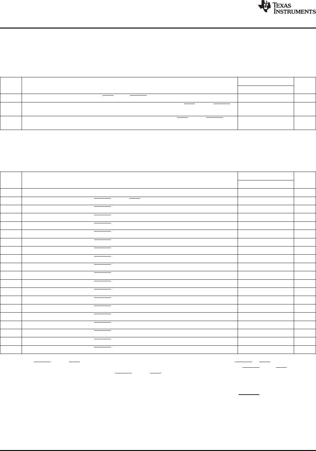
Table 7-21. Timing Requirements for Reset (see Figure 7-19 and Figure 7-20)
-1G
NO. UNIT
MIN MAX
1 t
w(RESET)
Pulse duration, POR low or RESET low 12C
(1)
ns
Setup time, boot and configuration pins valid before POR high or RESET
2 t
su(CONFIG)
12C
(1)
ns
high
(2)
Hold time, boot and configuration pins valid after POR high or RESET
3 t
h(CONFIG)
0 ns
high
(2)
(1) C = 1/DEV_MXI clock frequency in ns. The device clock source must be stable and at a valid frequency prior to meeting the t
w(RESET)
requirement.
(2) For the list of boot and configuration pins, see Table 3-5, Boot Terminal Functions.
Table 7-22. Switching Characteristics Over Recommended Operating Conditions During Reset
(1)
(see Figure 7-20)
-1G
NO. PARAMETER UNIT
MIN MAX
4 t
w(PAUSE)
Pulse duration, SYSCLKs paused (low) 10C 10C ns
23 t
d(RSTH-PAUSE)
Delay time, RESET high or POR high to SYSCLKs paused (low) 1990C ns
5 t
d(RSTL-BOOTZ)
Delay time, RESET low to Boot Configuration Group high impedance 0 20 ns
6 t
d(RSTL-DDRZZ)
Delay time, RESET low to DDR2 Z Group high impedance 0 7P + 20 ns
7 t
d(RSTL-DDRLL)
Delay time, RESET low to DDR2 Low Group low 0 3P + 20 ns
8 t
d(RSTL-DDRHH)
Delay time, RESET low to DDR2 High Group high 0 20 ns
13 t
d(RSTL-DDRZHZ)
Delay time, RESET low to DDR2 Z/High Group high impedance 0 7P + 20 ns
14 t
d(RSTL-DDRLHL)
Delay time, RESET low to DDR2 Low/High Group low 0 20 ns
17 t
d(RSTL-ZZ)
Delay time, RESET low to Z Group high impedance 0 20 ns
18 t
d(RSTL-LOWL)
Delay time, RESET low to Low Group low 0 20 ns
19 t
d(RSTL-HIGHH)
Delay time, RESET low to High Group high 0 20 ns
9 t
d(RSTL-BOOTV)
Delay time, RESET high to Boot Configuration Group valid
(2)
ns
10 t
d(RSTH-DDRZV)
Delay time, RESET high to DDR2 Z Group valid
(2)
ns
11 t
d(RSTH-DDRLV)
Delay time, RESET high to DDR2 Low Group valid
(2)
ns
12 t
d(RSTH-DDRHV)
Delay time, RESET high to DDR2 High Group valid
(2)
ns
15 t
d(RSTH-DDRZHV)
Delay time, RESET high to DDR2 Z/High Group valid high
(2)
ns
16 t
d(RSTH-DDRLHV)
Delay time, RESET high to DDR2 Low/High Group valid high
(2)
ns
20 t
d(RSTH-ZV)
Delay time, RESET high to Z Group valid
(2)
ns
21 t
d(RSTH-LOWV)
Delay time, RESET high to Low Group valid
(2)
ns
22 t
d(RSTH-HIGHV)
Delay time, RESET high to High Group valid
(2)
ns
(1) C = 1/DEV_CLKIN clock frequency in ns.
(2) Following RESET high or POR high, this signal group maintains the state the pins(s) achieved while RESET or POR was driven low until
the peripheral is enabled via the PSC. For example, the DDR2 Z Group goes high impedance following RESET low or POR low and
remains in the high-impedance state following RESET high or POR high until the DDR2 controller is enabled via the PSC.
Figure 7-19 shows the Power-Up Timing. Figure 7-20 shows the Warm Reset (RESET) Timing. Max Reset
Timing is identical to Warm Reset Timing, except the boot and configuration pins are not relatched and
the BOOTCFG register retains its previous value latched before the Max Reset was initiated.
190 Peripheral Information and Electrical Specifications Copyright © 2009–2012, Texas Instruments Incorporated
Submit Documentation Feedback
Product Folder Link(s): TMS320DM6467T