
Datasheet


Table Of Contents
- 1 Digital Media System-on-Chip (DMSoC)
- Table of Contents
- 2 Revision History
- 3 Device Overview
- 3.1 Device Characteristics
- 3.2 Device Compatibility
- 3.3 ARM Subsystem
- 3.3.1 ARM926EJ-S RISC CPU
- 3.3.2 CP15
- 3.3.3 MMU
- 3.3.4 Caches and Write Buffer
- 3.3.5 Tightly Coupled Memory (TCM)
- 3.3.6 Advanced High-Performance Bus (AHB)
- 3.3.7 Embedded Trace Macrocell (ETM) and Embedded Trace Buffer (ETB)
- 3.3.8 ARM Memory Mapping
- 3.3.9 Peripherals
- 3.3.10 PLL Controller (PLLC)
- 3.3.11 Power and Sleep Controller (PSC)
- 3.3.12 ARM Interrupt Controller (AINTC)
- 3.3.13 System Module
- 3.3.14 Power Management
- 3.4 DSP Subsystem
- 3.5 Memory Map Summary
- 3.6 Pin Assignments
- 3.7 Terminal Functions
- 3.8 Device Support
- 3.9 Documentation Support
- 3.10 Community Resources
- 4 Device Configurations
- 4.1 System Module Registers
- 4.2 Power Considerations
- 4.3 Clock Considerations
- 4.4 Boot Sequence
- 4.5 Configurations At Reset
- 4.6 Configurations After Reset
- 4.7 Multiplexed Pin Configurations
- 4.7.1 Pin Muxing Selection At Reset
- 4.7.2 Pin Muxing Selection After Reset
- 4.7.3 Pin Multiplexing Details
- 4.7.3.1 PCI, HPI, EMIFA, and ATA Pin Muxing
- 4.7.3.2 PWM Signal Muxing
- 4.7.3.3 TSIF0 Input Signal Muxing (Serial/Parallel)
- 4.7.3.4 TSIF0 Output Signal Muxing (Serial/Parallel)
- 4.7.3.5 TSIF1 Input Signal Muxing (Serial Only)
- 4.7.3.6 TSIF1 Output Signal Muxing (Serial Only)
- 4.7.3.7 CRGEN Signal Muxing
- 4.7.3.8 UART0 Pin Muxing
- 4.7.3.9 UART1 Pin Muxing
- 4.7.3.10 UART2 Pin Muxing
- 4.7.3.11 ARM/DSP Communications Interrupts
- 4.7.3.12 Emulation Control
- 4.8 Debugging Considerations
- 5 System Interconnect
- 6 Device Operating Conditions
- 7 Peripheral Information and Electrical Specifications
- 7.1 Parameter Information
- 7.2 Recommended Clock and Control Signal Transition Behavior
- 7.3 Power Supplies
- 7.4 External Clock Input From DEV_MXI/DEV_CLKIN and AUX_MXI/AUX_CLKIN Pins
- 7.5 Clock PLLs
- 7.6 Enhanced Direct Memory Access (EDMA3) Controller
- 7.7 Reset
- 7.8 Interrupts
- 7.9 External Memory Interface (EMIF)
- 7.10 DDR2 Memory Controller
- 7.10.1 DDR2 Memory Controller Electrical Data/Timing
- 7.10.2 DDR2 Interface
- 7.10.2.1 DDR2 Interface Schematic
- 7.10.2.2 Compatible JEDEC DDR2 Devices
- 7.10.2.3 PCB Stackup
- 7.10.2.4 Placement
- 7.10.2.5 DDR2 Keep Out Region
- 7.10.2.6 Bulk Bypass Capacitors
- 7.10.2.7 High-Speed Bypass Capacitors
- 7.10.2.8 Net Classes
- 7.10.2.9 DDR2 Signal Termination
- 7.10.2.10 VREF Routing
- 7.10.2.11 DDR2 CK and ADDR_CTRL Routing
- 7.11 Video Port Interface (VPIF)
- 7.12 Transport Stream Interface (TSIF)
- 7.13 Clock Recovery Generator (CRGEN)
- 7.14 Video Data Conversion Engine (VDCE)
- 7.15 Peripheral Component Interconnect (PCI)
- 7.16 Ethernet MAC (EMAC)
- 7.17 Management Data Input/Output (MDIO)
- 7.18 Host-Port Interface (HPI) Peripheral
- 7.19 USB 2.0 [see Note]
- 7.20 ATA Controller
- 7.21 VLYNQ
- 7.22 Multichannel Audio Serial Port (McASP0/1) Peripherals
- 7.23 Serial Peripheral Interface (SPI)
- 7.24 Universal Asynchronouse Receiver/Transmitter (UART)
- 7.25 Inter-Integrated Circuit (I2C)
- 7.26 Pulse Width Modulator (PWM)
- 7.27 Timers
- 7.28 General-Purpose Input/Output (GPIO)
- 7.29 IEEE 1149.1 JTAG
- 8 Mechanical Packaging and Orderable Information
TMS320DM6467T
SPRS605C –JULY 2009–REVISED JUNE 2012
www.ti.com
• Maximum Reset
• Warm Reset
• System Reset
7.7.7.1 Reset Type Status (RSTYPE) Register
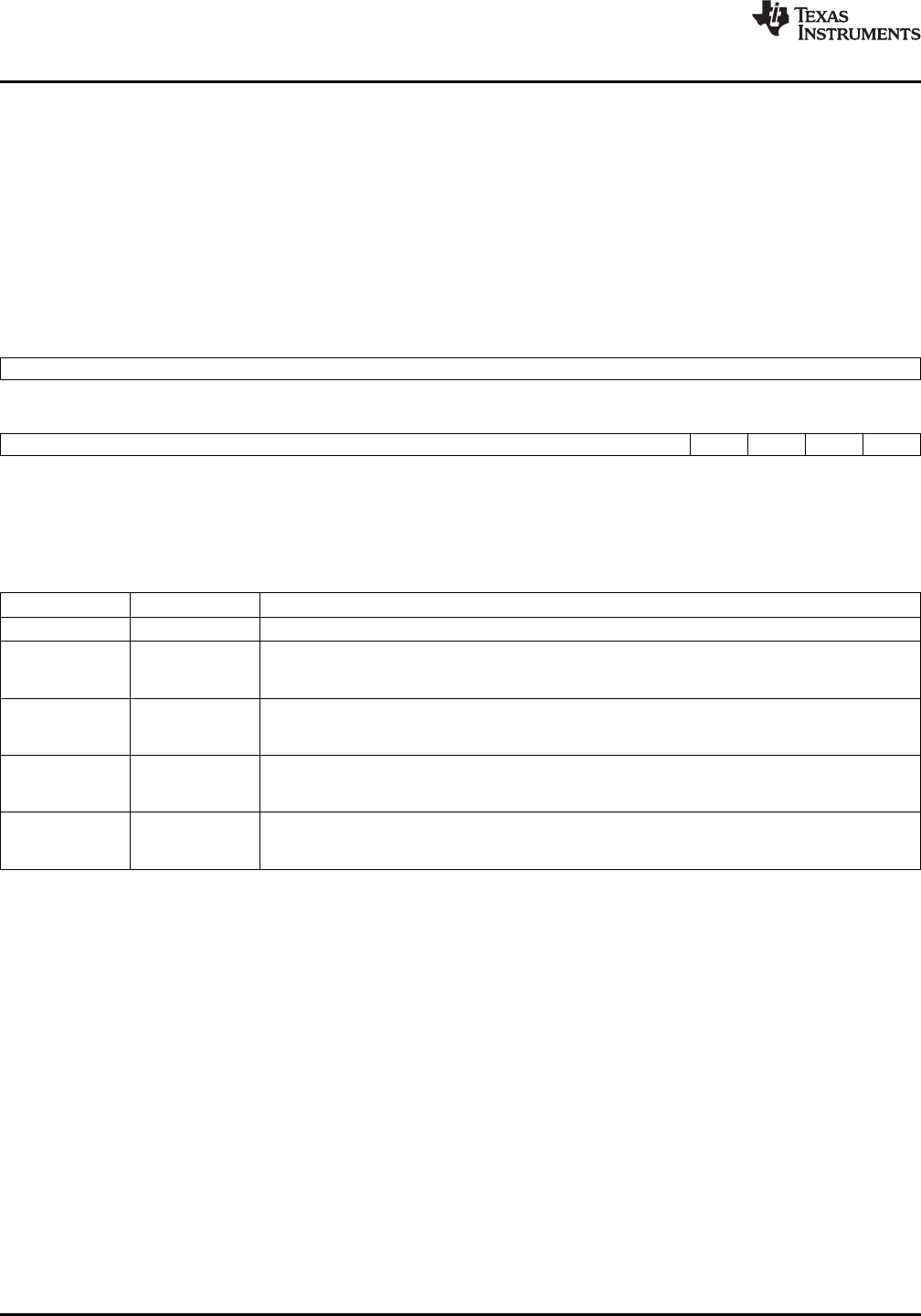
The Reset Type Status (RSTYPE) register (0x01C4 08E4) is the only register for the reset controller. This
register falls in the same memory range as the PLL1 controller registers (see Table 7-11 for the PLL1
Controller Registers (Including Reset Controller)). For more details on the RSTYPE register and its bit
descriptions, see Figure 7-18 and Table 7-20.
31 16
RESERVED
R-0000 0000 0000 0000
15 4 3 2 1 0
RESERVED SRST MRST WRST POR
R-0000 0000 0000 R-0/1 R-0/1 R-0/1 R-0/1
LEGEND: R = Read only; -n = value after reset
Figure 7-18. Reset Type Status (RSTYPE) Register [0x01C4 08E4]
Table 7-20. RSTYPE Register Bit Descriptions
BIT NAME DESCRIPTION
30:4 RESERVED Reserved. Read returns "0". Writes have no effect.
System Reset.
3 SRST 0 = System Reset was not the last reset to occur.
1 = System Reset was the last reset to occur.
Max Reset.
2 MRST 0 = Max Reset was not the last reset to occur.
1 = Max Reset was the last reset to occur.
Warm Reset.
1 WRST 0 = Warm Reset was not the last reset to occur.
1 = Warm Reset was the last reset to occur.
Power-on Reset.
0 POR 0 = Power-on Reset was not the last reset to occur.
1 = Power-on Reset was the last reset to occur.
7.7.8 Pin Behaviors at Reset
During normal operations, pins are controlled by the respective peripheral selected in the PINMUX0 or
PINMUX1 register. During device level global reset, the pin behaves as follows:
Multiplexed Boot and Configuration Pins
These pins are forced 3-stated when the device is in reset. This is to ensure the proper boot and
configuration values can be latched on these multiplexed pins. This is particularly useful in the case where
the boot and configuration values are driven by an external control device. Once the device is out of reset,
these pins are controlled by their respective default peripheral.
• Boot and Configuration Pins Group: VP_DOUT6/DSPBOOT, VP_DOUT5/PCIEN,
VP_DOUT4/CS2BW, VP_DOUT3/BTMODE3, VP_DOUT2/BTMODE2, VP_DOUT1/BTMODE1, and
VP_DOUT0/BTMODE0.
For information on whether external pullup/pulldown resistors should be used on the boot and
configuration pins, see Section 4.8.1, Pullup/Pulldown Resistors.
186 Peripheral Information and Electrical Specifications Copyright © 2009–2012, Texas Instruments Incorporated
Submit Documentation Feedback
Product Folder Link(s): TMS320DM6467T