
Datasheet


Table Of Contents
- 1 Digital Media System-on-Chip (DMSoC)
- Table of Contents
- 2 Revision History
- 3 Device Overview
- 3.1 Device Characteristics
- 3.2 Device Compatibility
- 3.3 ARM Subsystem
- 3.3.1 ARM926EJ-S RISC CPU
- 3.3.2 CP15
- 3.3.3 MMU
- 3.3.4 Caches and Write Buffer
- 3.3.5 Tightly Coupled Memory (TCM)
- 3.3.6 Advanced High-Performance Bus (AHB)
- 3.3.7 Embedded Trace Macrocell (ETM) and Embedded Trace Buffer (ETB)
- 3.3.8 ARM Memory Mapping
- 3.3.9 Peripherals
- 3.3.10 PLL Controller (PLLC)
- 3.3.11 Power and Sleep Controller (PSC)
- 3.3.12 ARM Interrupt Controller (AINTC)
- 3.3.13 System Module
- 3.3.14 Power Management
- 3.4 DSP Subsystem
- 3.5 Memory Map Summary
- 3.6 Pin Assignments
- 3.7 Terminal Functions
- 3.8 Device Support
- 3.9 Documentation Support
- 3.10 Community Resources
- 4 Device Configurations
- 4.1 System Module Registers
- 4.2 Power Considerations
- 4.3 Clock Considerations
- 4.4 Boot Sequence
- 4.5 Configurations At Reset
- 4.6 Configurations After Reset
- 4.7 Multiplexed Pin Configurations
- 4.7.1 Pin Muxing Selection At Reset
- 4.7.2 Pin Muxing Selection After Reset
- 4.7.3 Pin Multiplexing Details
- 4.7.3.1 PCI, HPI, EMIFA, and ATA Pin Muxing
- 4.7.3.2 PWM Signal Muxing
- 4.7.3.3 TSIF0 Input Signal Muxing (Serial/Parallel)
- 4.7.3.4 TSIF0 Output Signal Muxing (Serial/Parallel)
- 4.7.3.5 TSIF1 Input Signal Muxing (Serial Only)
- 4.7.3.6 TSIF1 Output Signal Muxing (Serial Only)
- 4.7.3.7 CRGEN Signal Muxing
- 4.7.3.8 UART0 Pin Muxing
- 4.7.3.9 UART1 Pin Muxing
- 4.7.3.10 UART2 Pin Muxing
- 4.7.3.11 ARM/DSP Communications Interrupts
- 4.7.3.12 Emulation Control
- 4.8 Debugging Considerations
- 5 System Interconnect
- 6 Device Operating Conditions
- 7 Peripheral Information and Electrical Specifications
- 7.1 Parameter Information
- 7.2 Recommended Clock and Control Signal Transition Behavior
- 7.3 Power Supplies
- 7.4 External Clock Input From DEV_MXI/DEV_CLKIN and AUX_MXI/AUX_CLKIN Pins
- 7.5 Clock PLLs
- 7.6 Enhanced Direct Memory Access (EDMA3) Controller
- 7.7 Reset
- 7.8 Interrupts
- 7.9 External Memory Interface (EMIF)
- 7.10 DDR2 Memory Controller
- 7.10.1 DDR2 Memory Controller Electrical Data/Timing
- 7.10.2 DDR2 Interface
- 7.10.2.1 DDR2 Interface Schematic
- 7.10.2.2 Compatible JEDEC DDR2 Devices
- 7.10.2.3 PCB Stackup
- 7.10.2.4 Placement
- 7.10.2.5 DDR2 Keep Out Region
- 7.10.2.6 Bulk Bypass Capacitors
- 7.10.2.7 High-Speed Bypass Capacitors
- 7.10.2.8 Net Classes
- 7.10.2.9 DDR2 Signal Termination
- 7.10.2.10 VREF Routing
- 7.10.2.11 DDR2 CK and ADDR_CTRL Routing
- 7.11 Video Port Interface (VPIF)
- 7.12 Transport Stream Interface (TSIF)
- 7.13 Clock Recovery Generator (CRGEN)
- 7.14 Video Data Conversion Engine (VDCE)
- 7.15 Peripheral Component Interconnect (PCI)
- 7.16 Ethernet MAC (EMAC)
- 7.17 Management Data Input/Output (MDIO)
- 7.18 Host-Port Interface (HPI) Peripheral
- 7.19 USB 2.0 [see Note]
- 7.20 ATA Controller
- 7.21 VLYNQ
- 7.22 Multichannel Audio Serial Port (McASP0/1) Peripherals
- 7.23 Serial Peripheral Interface (SPI)
- 7.24 Universal Asynchronouse Receiver/Transmitter (UART)
- 7.25 Inter-Integrated Circuit (I2C)
- 7.26 Pulse Width Modulator (PWM)
- 7.27 Timers
- 7.28 General-Purpose Input/Output (GPIO)
- 7.29 IEEE 1149.1 JTAG
- 8 Mechanical Packaging and Orderable Information
TMS320DM6467T
SPRS605C –JULY 2009–REVISED JUNE 2012
www.ti.com
7.7 Reset
The reset controller detects the different type of resets supported on the DM6467T device and manages
the distribution of those resets throughout the device.
The DM6467T device has several types of device-level global resets—power-on reset, warm reset, max
reset, and system reset. Table 7-19 explains further the types of reset, the reset initiator, and the effects of
each reset on the chip. See Section 7.7.9, Reset Electrical Data/Timing, for more information on the
effects of each reset on the PLL controllers and their clocks.
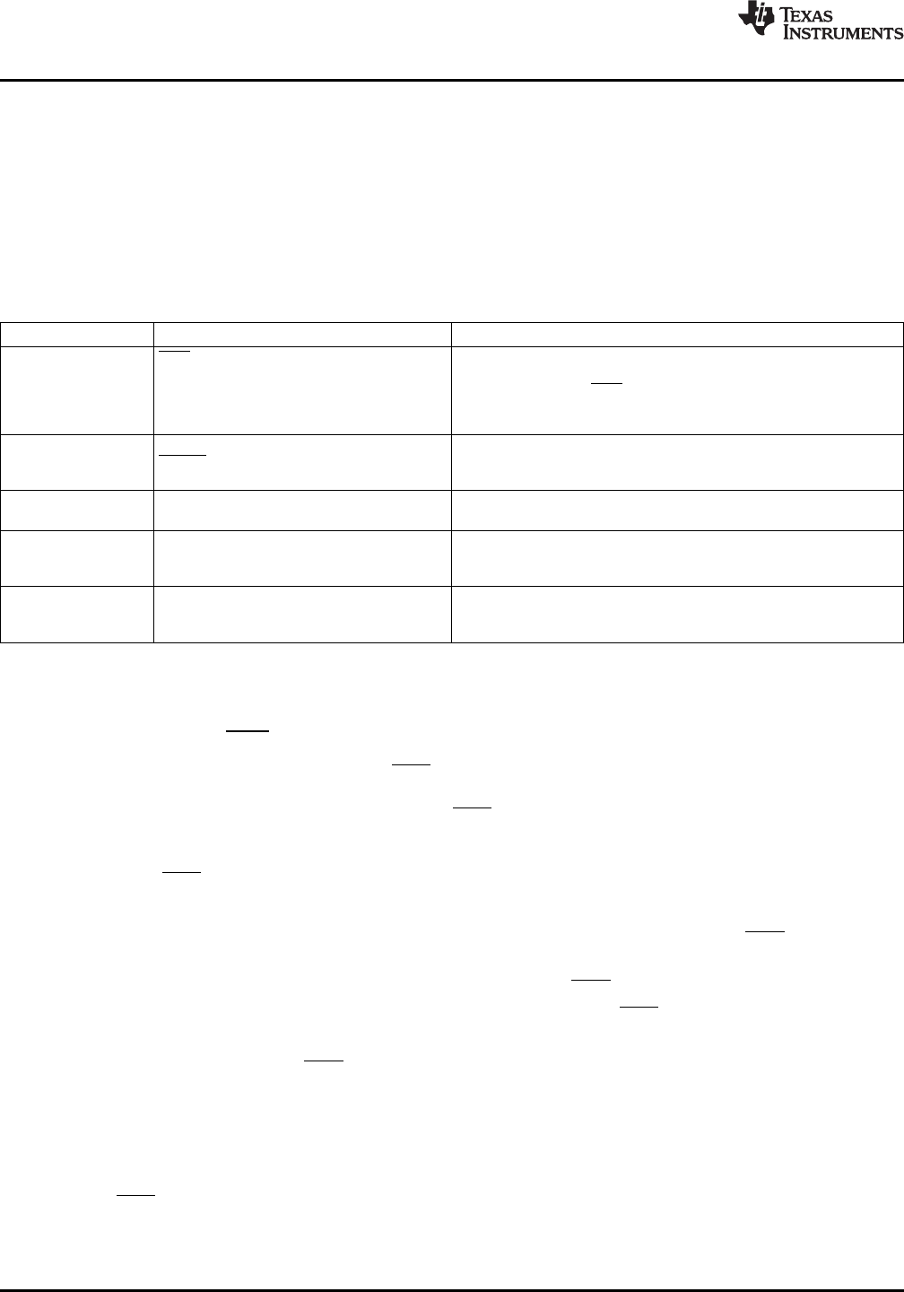
Table 7-19. Device-Level Global Reset Types
TYPE INITIATOR EFFECT(S)
POR pin Global chip reset (Cold reset). Activates the POR signal on chip,
which resets the entire chip including the emulation logic.
Power-on Reset
The power-on reset (POR) pin must be driven low during power
(POR)
ramp of the device.
Device boot and configuration pins are latched.
Resets everything except for the emulation logic. Emulator stays
Warm Reset RESET pin alive during Warm Reset.
Device boot and configuration pins are latched.
Same as a Warm Reset, except the DM6467T device boot and
Max Reset Emulator, WD Timer (Timer 2)
configuration pins are not re-latched.
A system reset maintains memory contents and does not reset the
System Reset Emulator test and emulation circuitry. The device boot and configuration pins
are also not re-latched.
MMR controls the C64x+ reset input. This is used for control of
C64x+ Local Reset
Software (register bit) C64x+ reset by the ARM. The C64x+ Slave DMA port is still alive
(DSP Reset)
when in local reset.
In addition to device-level global resets, the PSC provides the capability to cause local resets to
peripherals and/or the C64x+ DSP.
7.7.1 Power-on Reset (POR Pin)
Power-on Reset (POR) is initiated by the POR pin and is used to reset the entire chip, including the test
and emulation logic. Power-on Reset is also referred to as a cold reset since the device usually goes
through a power-up cycle. During power-up, the POR pin must be asserted (driven low) until the power
supplies have reached their normal operating conditions. If an external oscillator is used on the
DEV_MXI/DEV_CLKIN pin, the source clock should also be running at the correct frequency prior to de-
asserting the POR pin. Note: A device power-up cycle is not required to initiate a Power-on Reset.
The following sequence must be followed during a Power-on Reset.
1. Wait for the power supplies to reach normal operating conditions while keeping the POR pin asserted
(driven low).
2. Wait for the input clock source to be stable while keeping the POR pin asserted (low).
3. Once the power supplies and the input clock source are stable, the POR pin must remain asserted
(low) for a minimum of 12 DEV_MXI cycles.
Within the low period of the POR pin, the following happens:
– The reset signals flow to the entire chip (including the test and emulation logic), resetting the
modules on chip.
– The PLL Controller clocks start at the frequency of the DEV_MXI clock. The clocks are propagated
throughout the chip to reset the chip synchronously. By default, both PLL1 and PLL2 are in reset
and unlocked. The PLL Controllers default to PLL Bypass Mode.
4. The POR pin may now be deasserted (driven high).
182 Peripheral Information and Electrical Specifications Copyright © 2009–2012, Texas Instruments Incorporated
Submit Documentation Feedback
Product Folder Link(s): TMS320DM6467T