
Datasheet


Table Of Contents
- 1 Digital Media System-on-Chip (DMSoC)
- Table of Contents
- 2 Revision History
- 3 Device Overview
- 3.1 Device Characteristics
- 3.2 Device Compatibility
- 3.3 ARM Subsystem
- 3.3.1 ARM926EJ-S RISC CPU
- 3.3.2 CP15
- 3.3.3 MMU
- 3.3.4 Caches and Write Buffer
- 3.3.5 Tightly Coupled Memory (TCM)
- 3.3.6 Advanced High-Performance Bus (AHB)
- 3.3.7 Embedded Trace Macrocell (ETM) and Embedded Trace Buffer (ETB)
- 3.3.8 ARM Memory Mapping
- 3.3.9 Peripherals
- 3.3.10 PLL Controller (PLLC)
- 3.3.11 Power and Sleep Controller (PSC)
- 3.3.12 ARM Interrupt Controller (AINTC)
- 3.3.13 System Module
- 3.3.14 Power Management
- 3.4 DSP Subsystem
- 3.5 Memory Map Summary
- 3.6 Pin Assignments
- 3.7 Terminal Functions
- 3.8 Device Support
- 3.9 Documentation Support
- 3.10 Community Resources
- 4 Device Configurations
- 4.1 System Module Registers
- 4.2 Power Considerations
- 4.3 Clock Considerations
- 4.4 Boot Sequence
- 4.5 Configurations At Reset
- 4.6 Configurations After Reset
- 4.7 Multiplexed Pin Configurations
- 4.7.1 Pin Muxing Selection At Reset
- 4.7.2 Pin Muxing Selection After Reset
- 4.7.3 Pin Multiplexing Details
- 4.7.3.1 PCI, HPI, EMIFA, and ATA Pin Muxing
- 4.7.3.2 PWM Signal Muxing
- 4.7.3.3 TSIF0 Input Signal Muxing (Serial/Parallel)
- 4.7.3.4 TSIF0 Output Signal Muxing (Serial/Parallel)
- 4.7.3.5 TSIF1 Input Signal Muxing (Serial Only)
- 4.7.3.6 TSIF1 Output Signal Muxing (Serial Only)
- 4.7.3.7 CRGEN Signal Muxing
- 4.7.3.8 UART0 Pin Muxing
- 4.7.3.9 UART1 Pin Muxing
- 4.7.3.10 UART2 Pin Muxing
- 4.7.3.11 ARM/DSP Communications Interrupts
- 4.7.3.12 Emulation Control
- 4.8 Debugging Considerations
- 5 System Interconnect
- 6 Device Operating Conditions
- 7 Peripheral Information and Electrical Specifications
- 7.1 Parameter Information
- 7.2 Recommended Clock and Control Signal Transition Behavior
- 7.3 Power Supplies
- 7.4 External Clock Input From DEV_MXI/DEV_CLKIN and AUX_MXI/AUX_CLKIN Pins
- 7.5 Clock PLLs
- 7.6 Enhanced Direct Memory Access (EDMA3) Controller
- 7.7 Reset
- 7.8 Interrupts
- 7.9 External Memory Interface (EMIF)
- 7.10 DDR2 Memory Controller
- 7.10.1 DDR2 Memory Controller Electrical Data/Timing
- 7.10.2 DDR2 Interface
- 7.10.2.1 DDR2 Interface Schematic
- 7.10.2.2 Compatible JEDEC DDR2 Devices
- 7.10.2.3 PCB Stackup
- 7.10.2.4 Placement
- 7.10.2.5 DDR2 Keep Out Region
- 7.10.2.6 Bulk Bypass Capacitors
- 7.10.2.7 High-Speed Bypass Capacitors
- 7.10.2.8 Net Classes
- 7.10.2.9 DDR2 Signal Termination
- 7.10.2.10 VREF Routing
- 7.10.2.11 DDR2 CK and ADDR_CTRL Routing
- 7.11 Video Port Interface (VPIF)
- 7.12 Transport Stream Interface (TSIF)
- 7.13 Clock Recovery Generator (CRGEN)
- 7.14 Video Data Conversion Engine (VDCE)
- 7.15 Peripheral Component Interconnect (PCI)
- 7.16 Ethernet MAC (EMAC)
- 7.17 Management Data Input/Output (MDIO)
- 7.18 Host-Port Interface (HPI) Peripheral
- 7.19 USB 2.0 [see Note]
- 7.20 ATA Controller
- 7.21 VLYNQ
- 7.22 Multichannel Audio Serial Port (McASP0/1) Peripherals
- 7.23 Serial Peripheral Interface (SPI)
- 7.24 Universal Asynchronouse Receiver/Transmitter (UART)
- 7.25 Inter-Integrated Circuit (I2C)
- 7.26 Pulse Width Modulator (PWM)
- 7.27 Timers
- 7.28 General-Purpose Input/Output (GPIO)
- 7.29 IEEE 1149.1 JTAG
- 8 Mechanical Packaging and Orderable Information
TMS320DM6467T
SPRS605C –JULY 2009–REVISED JUNE 2012
www.ti.com
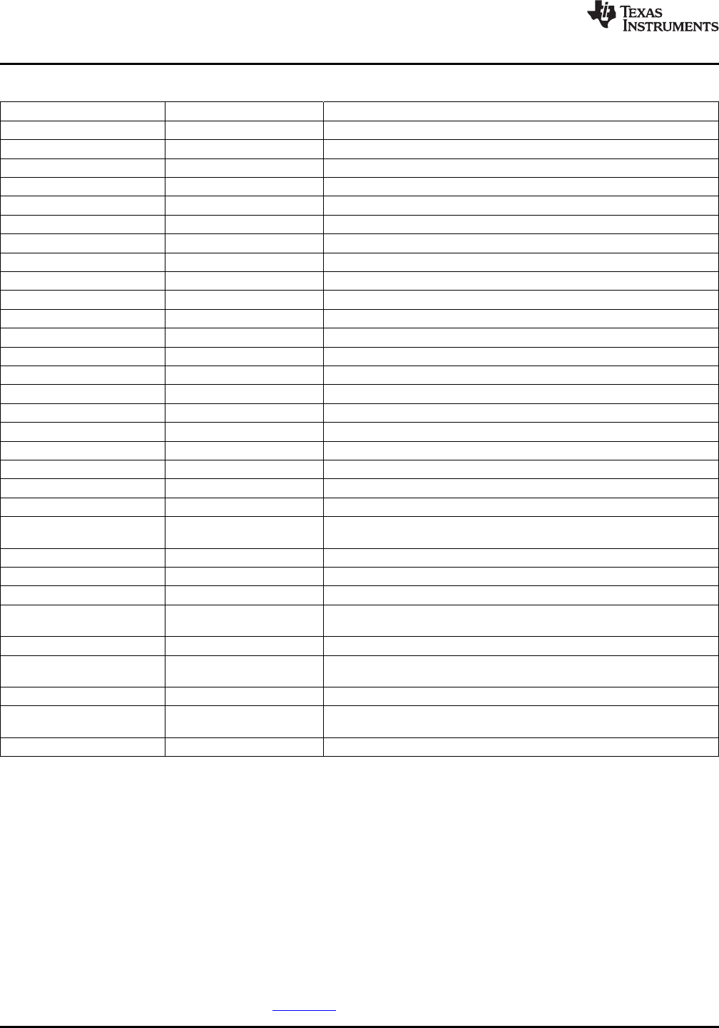
Table 3-2. C64x+ Cache Registers (continued)
HEX ADDRESS RANGE REGISTER ACRONYM DESCRIPTION
0x0184 401C L2IWC L2 invalidate word count register
0x0184 4020 L1PIBAR L1P invalidate base address register
0x0184 4024 L1PIWC L1P invalidate word count register
0x0184 4030 L1DWIBAR L1D writeback invalidate base address register
0x0184 4034 L1DWIWC L1D writeback invalidate word count register
0x0184 4038 - Reserved
0x0184 4040 L1DWBAR L1D Block Writeback
0x0184 4044 L1DWWC L1D Block Writeback
0x0184 4048 L1DIBAR L1D invalidate base address register
0x0184 404C L1DIWC L1D invalidate word count register
0x0184 4050 - 0x0184 4FFF - Reserved
0x0184 5000 L2WB L2 writeback all register
0x0184 5004 L2WBINV L2 writeback invalidate all register
0x0184 5008 L2INV L2 Global Invalidate without writeback
0x0184 500C - 0x0184 5027 - Reserved
0x0184 5028 L1PINV L1P Global Invalidate
0x0184 502C - 0x0184 5039 - Reserved
0x0184 5040 L1DWB L1D Global Writeback
0x0184 5044 L1DWBINV L1D Global Writeback with Invalidate
0x0184 5048 L1DINV L1D Global Invalidate without writeback
0x0184 8000 - 0x0184 803C MAR0 - MAR15 Reserved (corresponds to byte address 0x0000 0000 - 0x0FFF FFFF)
Memory Attribute Registers for ARM TCM (corresponds to byte address
0x0184 8040 MAR16
0x1000 0000 - 0x10FF FFFF)
0x0184 8044 - 0x0184 80FC MAR17 - MAR63 Reserved (corresponds to byte address 0x1100 0000 - 0x3FFF FFFF)
0x0184 8100 MAR64 Reserved (corresponds to byte address 0x4000 0000 - 0x40FF FFFF)
0x0184 8104 MAR65 Reserved (corresponds to byte address 0x4100 0000 - 0x41FF FFFF)
Memory Attribute Registers for EMIFA (corresponds to byte address 0x4200
0x0184 8108 - 0x0184 8124 MAR66 - MAR73
0000 - 0x49FF FFFF)
0x0184 8128 - 0x0184 812C MAR74 - MAR75 Reserved (corresponds to byte address 0x4A00 0000 - 0x4BFF FFFF)
Memory Attribute Registers for VLYNQ (corresponds to byte address
0x0184 8130 - 0x0184 813C MAR76 - MAR79
0x4C00 0000 - 0x4FFF FFFF)
0x0184 8140 - 0x0184 81FC MAR80 - MAR127 Reserved (corresponds to byte address 0x5000 0000 - 0x7FFF FFFF)
Memory Attribute Registers for DDR2 (corresponds to byte address 0x8000
0x0184 8200 - 0x0184 82FC MAR128 - MAR191
0000 - 0xBFFF FFFF)
0x0184 8300 - 0x0184 83FC MAR192 - MAR255 Reserved (corresponds to byte address 0xC000 0000 - 0xFFFF FFFF)
3.4.3 Peripherals
The DSP has access/controllability of the following peripherals:
• HDVICP0/1
• EDMA
• McASP0/1
• 2 Timers (Timer0 and Timer1) that can each be configured as 1 64-bit or 2 32-bit timers
3.4.4 DSP Interrupt Controller
The DSP Interrupt Controller accepts device interrupts and appropriately maps them to the DSP’s
available interrupts. The DSP Interrupt Controller is briefly described in this document in the Interrupts
section. For more detailed on the DSP Interrupt Controller, see the TMS320C64x+ DSP Megamodule
Reference Guide (literature number SPRU871).
18 Device Overview Copyright © 2009–2012, Texas Instruments Incorporated
Submit Documentation Feedback
Product Folder Link(s): TMS320DM6467T