
Datasheet


Table Of Contents
- 1 Digital Media System-on-Chip (DMSoC)
- Table of Contents
- 2 Revision History
- 3 Device Overview
- 3.1 Device Characteristics
- 3.2 Device Compatibility
- 3.3 ARM Subsystem
- 3.3.1 ARM926EJ-S RISC CPU
- 3.3.2 CP15
- 3.3.3 MMU
- 3.3.4 Caches and Write Buffer
- 3.3.5 Tightly Coupled Memory (TCM)
- 3.3.6 Advanced High-Performance Bus (AHB)
- 3.3.7 Embedded Trace Macrocell (ETM) and Embedded Trace Buffer (ETB)
- 3.3.8 ARM Memory Mapping
- 3.3.9 Peripherals
- 3.3.10 PLL Controller (PLLC)
- 3.3.11 Power and Sleep Controller (PSC)
- 3.3.12 ARM Interrupt Controller (AINTC)
- 3.3.13 System Module
- 3.3.14 Power Management
- 3.4 DSP Subsystem
- 3.5 Memory Map Summary
- 3.6 Pin Assignments
- 3.7 Terminal Functions
- 3.8 Device Support
- 3.9 Documentation Support
- 3.10 Community Resources
- 4 Device Configurations
- 4.1 System Module Registers
- 4.2 Power Considerations
- 4.3 Clock Considerations
- 4.4 Boot Sequence
- 4.5 Configurations At Reset
- 4.6 Configurations After Reset
- 4.7 Multiplexed Pin Configurations
- 4.7.1 Pin Muxing Selection At Reset
- 4.7.2 Pin Muxing Selection After Reset
- 4.7.3 Pin Multiplexing Details
- 4.7.3.1 PCI, HPI, EMIFA, and ATA Pin Muxing
- 4.7.3.2 PWM Signal Muxing
- 4.7.3.3 TSIF0 Input Signal Muxing (Serial/Parallel)
- 4.7.3.4 TSIF0 Output Signal Muxing (Serial/Parallel)
- 4.7.3.5 TSIF1 Input Signal Muxing (Serial Only)
- 4.7.3.6 TSIF1 Output Signal Muxing (Serial Only)
- 4.7.3.7 CRGEN Signal Muxing
- 4.7.3.8 UART0 Pin Muxing
- 4.7.3.9 UART1 Pin Muxing
- 4.7.3.10 UART2 Pin Muxing
- 4.7.3.11 ARM/DSP Communications Interrupts
- 4.7.3.12 Emulation Control
- 4.8 Debugging Considerations
- 5 System Interconnect
- 6 Device Operating Conditions
- 7 Peripheral Information and Electrical Specifications
- 7.1 Parameter Information
- 7.2 Recommended Clock and Control Signal Transition Behavior
- 7.3 Power Supplies
- 7.4 External Clock Input From DEV_MXI/DEV_CLKIN and AUX_MXI/AUX_CLKIN Pins
- 7.5 Clock PLLs
- 7.6 Enhanced Direct Memory Access (EDMA3) Controller
- 7.7 Reset
- 7.8 Interrupts
- 7.9 External Memory Interface (EMIF)
- 7.10 DDR2 Memory Controller
- 7.10.1 DDR2 Memory Controller Electrical Data/Timing
- 7.10.2 DDR2 Interface
- 7.10.2.1 DDR2 Interface Schematic
- 7.10.2.2 Compatible JEDEC DDR2 Devices
- 7.10.2.3 PCB Stackup
- 7.10.2.4 Placement
- 7.10.2.5 DDR2 Keep Out Region
- 7.10.2.6 Bulk Bypass Capacitors
- 7.10.2.7 High-Speed Bypass Capacitors
- 7.10.2.8 Net Classes
- 7.10.2.9 DDR2 Signal Termination
- 7.10.2.10 VREF Routing
- 7.10.2.11 DDR2 CK and ADDR_CTRL Routing
- 7.11 Video Port Interface (VPIF)
- 7.12 Transport Stream Interface (TSIF)
- 7.13 Clock Recovery Generator (CRGEN)
- 7.14 Video Data Conversion Engine (VDCE)
- 7.15 Peripheral Component Interconnect (PCI)
- 7.16 Ethernet MAC (EMAC)
- 7.17 Management Data Input/Output (MDIO)
- 7.18 Host-Port Interface (HPI) Peripheral
- 7.19 USB 2.0 [see Note]
- 7.20 ATA Controller
- 7.21 VLYNQ
- 7.22 Multichannel Audio Serial Port (McASP0/1) Peripherals
- 7.23 Serial Peripheral Interface (SPI)
- 7.24 Universal Asynchronouse Receiver/Transmitter (UART)
- 7.25 Inter-Integrated Circuit (I2C)
- 7.26 Pulse Width Modulator (PWM)
- 7.27 Timers
- 7.28 General-Purpose Input/Output (GPIO)
- 7.29 IEEE 1149.1 JTAG
- 8 Mechanical Packaging and Orderable Information
TMS320DM6467T
www.ti.com
SPRS605C –JULY 2009–REVISED JUNE 2012
3.4.2 DSP Memory Mapping
The DSP memory map is shown in Section 3.5, Memory Map Summary. Configuration of the control
registers for DDR2, EMIFA, and ARM Internal RAM is supported by the ARM. The DSP has access to
memories shown in the following sections.
3.4.2.1 ARM Internal Memories
The DSP has access to the 32KB ARM Internal RAM on the ARM D-TCM interface (i.e., data only).
3.4.2.2 External Memories
The DSP has access to the following External memories:
• DDR2 Synchronous DRAM
• Asynchronous EMIF / NOR Flash
• ATA
3.4.2.3 DSP Internal Memories
The DSP has access to the following DSP memories:
• L2 RAM
• L1P RAM
• L1D RAM
3.4.2.4 C64x+ CPU
The C64x+ core uses a two-level cache-based architecture. The Level 1 Program memory/cache (L1P)
consists of 32 KB memory space that can be configured as mapped memory or direct mapped cache. The
Level 1 Data memory/cache (L1D) consists of 32 KB that can be configured as mapped memory or 2-way
set associated cache. The Level 2 memory/cache (L2) consists of a 128 KB RAM memory space that is
shared between program and data space. L2 memory can be configured as mapped memory, cache, or a
combination of both.
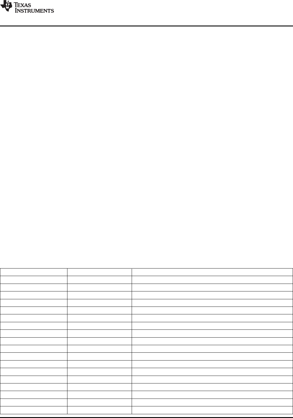
Table 3-2 shows a memory map of the C64x+ CPU cache registers for the device.
Table 3-2. C64x+ Cache Registers
HEX ADDRESS RANGE REGISTER ACRONYM DESCRIPTION
0x0184 0000 L2CFG L2 Cache configuration register
0x0184 0020 L1PCFG L1P Size Cache configuration register
0x0184 0024 L1PCC L1P Freeze Mode Cache configuration register
0x0184 0040 L1DCFG L1D Size Cache configuration register
0x0184 0044 L1DCC L1D Freeze Mode Cache configuration register
0x0184 0048 - 0x0184 0FFC - Reserved
0x0184 1000 EDMAWEIGHT L2 EDMA access control register
0x0184 1004 - 0x0184 1FFC - Reserved
0x0184 2000 L2ALLOC0 L2 allocation register 0
0x0184 2004 L2ALLOC1 L2 allocation register 1
0x0184 2008 L2ALLOC2 L2 allocation register 2
0x0184 200C L2ALLOC3 L2 allocation register 3
0x0184 2010 - 0x0184 3FFF - Reserved
0x0184 4000 L2WBAR L2 writeback base address register
0x0184 4004 L2WWC L2 writeback word count register
0x0184 4010 L2WIBAR L2 writeback invalidate base address register
0x0184 4014 L2WIWC L2 writeback invalidate word count register
0x0184 4018 L2IBAR L2 invalidate base address register
Copyright © 2009–2012, Texas Instruments Incorporated Device Overview 17
Submit Documentation Feedback
Product Folder Link(s): TMS320DM6467T