
Datasheet


Table Of Contents
- 1 Digital Media System-on-Chip (DMSoC)
- Table of Contents
- 2 Revision History
- 3 Device Overview
- 3.1 Device Characteristics
- 3.2 Device Compatibility
- 3.3 ARM Subsystem
- 3.3.1 ARM926EJ-S RISC CPU
- 3.3.2 CP15
- 3.3.3 MMU
- 3.3.4 Caches and Write Buffer
- 3.3.5 Tightly Coupled Memory (TCM)
- 3.3.6 Advanced High-Performance Bus (AHB)
- 3.3.7 Embedded Trace Macrocell (ETM) and Embedded Trace Buffer (ETB)
- 3.3.8 ARM Memory Mapping
- 3.3.9 Peripherals
- 3.3.10 PLL Controller (PLLC)
- 3.3.11 Power and Sleep Controller (PSC)
- 3.3.12 ARM Interrupt Controller (AINTC)
- 3.3.13 System Module
- 3.3.14 Power Management
- 3.4 DSP Subsystem
- 3.5 Memory Map Summary
- 3.6 Pin Assignments
- 3.7 Terminal Functions
- 3.8 Device Support
- 3.9 Documentation Support
- 3.10 Community Resources
- 4 Device Configurations
- 4.1 System Module Registers
- 4.2 Power Considerations
- 4.3 Clock Considerations
- 4.4 Boot Sequence
- 4.5 Configurations At Reset
- 4.6 Configurations After Reset
- 4.7 Multiplexed Pin Configurations
- 4.7.1 Pin Muxing Selection At Reset
- 4.7.2 Pin Muxing Selection After Reset
- 4.7.3 Pin Multiplexing Details
- 4.7.3.1 PCI, HPI, EMIFA, and ATA Pin Muxing
- 4.7.3.2 PWM Signal Muxing
- 4.7.3.3 TSIF0 Input Signal Muxing (Serial/Parallel)
- 4.7.3.4 TSIF0 Output Signal Muxing (Serial/Parallel)
- 4.7.3.5 TSIF1 Input Signal Muxing (Serial Only)
- 4.7.3.6 TSIF1 Output Signal Muxing (Serial Only)
- 4.7.3.7 CRGEN Signal Muxing
- 4.7.3.8 UART0 Pin Muxing
- 4.7.3.9 UART1 Pin Muxing
- 4.7.3.10 UART2 Pin Muxing
- 4.7.3.11 ARM/DSP Communications Interrupts
- 4.7.3.12 Emulation Control
- 4.8 Debugging Considerations
- 5 System Interconnect
- 6 Device Operating Conditions
- 7 Peripheral Information and Electrical Specifications
- 7.1 Parameter Information
- 7.2 Recommended Clock and Control Signal Transition Behavior
- 7.3 Power Supplies
- 7.4 External Clock Input From DEV_MXI/DEV_CLKIN and AUX_MXI/AUX_CLKIN Pins
- 7.5 Clock PLLs
- 7.6 Enhanced Direct Memory Access (EDMA3) Controller
- 7.7 Reset
- 7.8 Interrupts
- 7.9 External Memory Interface (EMIF)
- 7.10 DDR2 Memory Controller
- 7.10.1 DDR2 Memory Controller Electrical Data/Timing
- 7.10.2 DDR2 Interface
- 7.10.2.1 DDR2 Interface Schematic
- 7.10.2.2 Compatible JEDEC DDR2 Devices
- 7.10.2.3 PCB Stackup
- 7.10.2.4 Placement
- 7.10.2.5 DDR2 Keep Out Region
- 7.10.2.6 Bulk Bypass Capacitors
- 7.10.2.7 High-Speed Bypass Capacitors
- 7.10.2.8 Net Classes
- 7.10.2.9 DDR2 Signal Termination
- 7.10.2.10 VREF Routing
- 7.10.2.11 DDR2 CK and ADDR_CTRL Routing
- 7.11 Video Port Interface (VPIF)
- 7.12 Transport Stream Interface (TSIF)
- 7.13 Clock Recovery Generator (CRGEN)
- 7.14 Video Data Conversion Engine (VDCE)
- 7.15 Peripheral Component Interconnect (PCI)
- 7.16 Ethernet MAC (EMAC)
- 7.17 Management Data Input/Output (MDIO)
- 7.18 Host-Port Interface (HPI) Peripheral
- 7.19 USB 2.0 [see Note]
- 7.20 ATA Controller
- 7.21 VLYNQ
- 7.22 Multichannel Audio Serial Port (McASP0/1) Peripherals
- 7.23 Serial Peripheral Interface (SPI)
- 7.24 Universal Asynchronouse Receiver/Transmitter (UART)
- 7.25 Inter-Integrated Circuit (I2C)
- 7.26 Pulse Width Modulator (PWM)
- 7.27 Timers
- 7.28 General-Purpose Input/Output (GPIO)
- 7.29 IEEE 1149.1 JTAG
- 8 Mechanical Packaging and Orderable Information
TMS320DM6467T
SPRS605C –JULY 2009–REVISED JUNE 2012
www.ti.com
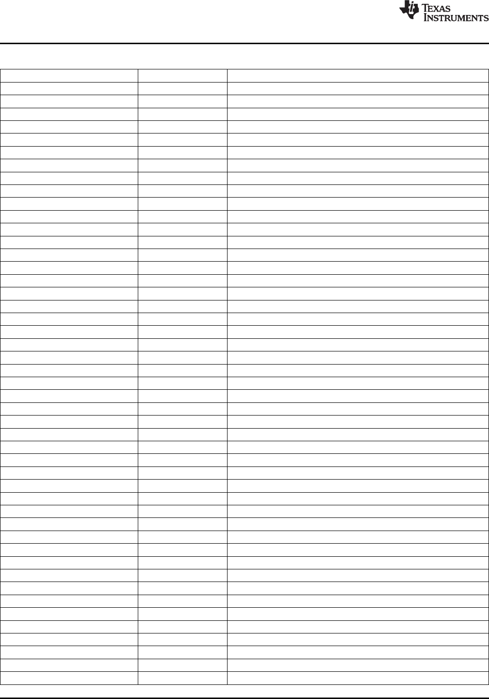
Table 7-16. DM6467T EDMA Registers (continued)
HEX ADDRESS RANGE ACRONYM REGISTER NAME
0x01C0 0440 Q1E0 Event Q1 Entry 0 Register
0x01C0 0444 Q1E1 Event Q1 Entry 1 Register
0x01C0 0448 Q1E2 Event Q1 Entry 2 Register
0x01C0 044C Q1E3 Event Q1 Entry 3 Register
0x01C0 0450 Q1E4 Event Q1 Entry 4 Register
0x01C0 0454 Q1E5 Event Q1 Entry 5 Register
0x01C0 0458 Q1E6 Event Q1 Entry 6 Register
0x01C0 045C Q1E7 Event Q1 Entry 7 Register
0x01C0 0460 Q1E8 Event Q1 Entry 8 Register
0x01C0 0464 Q1E9 Event Q1 Entry 9 Register
0x01C0 0468 Q1E10 Event Q1 Entry 10 Register
0x01C0 046C Q1E11 Event Q1 Entry 11 Register
0x01C0 0470 Q1E12 Event Q1 Entry 12 Register
0x01C0 0474 Q1E13 Event Q1 Entry 13 Register
0x01C0 0478 Q1E14 Event Q1 Entry 14 Register
0x01C0 047C Q1E15 Event Q1 Entry 15 Register
0x01C0 0480 Q2E0 Event Q2 Entry 0 Register
0x01C0 0484 Q2E1 Event Q2 Entry 1 Register
0x01C0 0488 Q2E2 Event Q2 Entry 2 Register
0x01C0 048C Q2E3 Event Q2 Entry 3 Register
0x01C0 0490 Q2E4 Event Q2 Entry 4 Register
0x01C0 0494 Q2E5 Event Q2 Entry 5 Register
0x01C0 0498 Q2E6 Event Q2 Entry 6 Register
0x01C0 049C Q2E7 Event Q2 Entry 7 Register
0x01C0 04A0 Q2E8 Event Q2 Entry 8 Register
0x01C0 04A4 Q2E9 Event Q2 Entry 9 Register
0x01C0 04A8 Q2E10 Event Q2 Entry 10 Register
0x01C0 04AC Q2E11 Event Q2 Entry 11 Register
0x01C0 04B0 Q2E12 Event Q2 Entry 12 Register
0x01C0 04B4 Q2E13 Event Q2 Entry 13 Register
0x01C0 04B8 Q2E14 Event Q2 Entry 14 Register
0x01C0 04BC Q2E15 Event Q2 Entry 15 Register
0x01C0 04C0 Q3E0 Event Q3 Entry 0 Register
0x01C0 04C4 Q3E1 Event Q3 Entry 1 Register
0x01C0 04C8 Q3E2 Event Q3 Entry 2 Register
0x01C0 04CC Q3E3 Event Q3 Entry 3 Register
0x01C0 04D0 Q3E4 Event Q3 Entry 4 Register
0x01C0 04D4 Q3E5 Event Q3 Entry 5 Register
0x01C0 04D8 Q3E6 Event Q3 Entry 6 Register
0x01C0 04DC Q3E7 Event Q3 Entry 7 Register
0x01C0 04E0 Q3E8 Event Q3 Entry 8 Register
0x01C0 04E4 Q3E9 Event Q3 Entry 9 Register
0x01C0 04E8 Q3E10 Event Q3 Entry 10 Register
0x01C0 04EC Q3E11 Event Q3 Entry 11 Register
0x01C0 04F0 Q3E12 Event Q3 Entry 12 Register
0x01C0 04F4 Q3E13 Event Q3 Entry 13 Register
0x01C0 04F8 Q3E14 Event Q3 Entry 14 Register
168 Peripheral Information and Electrical Specifications Copyright © 2009–2012, Texas Instruments Incorporated
Submit Documentation Feedback
Product Folder Link(s): TMS320DM6467T