
Datasheet


Table Of Contents
- 1 Digital Media System-on-Chip (DMSoC)
- Table of Contents
- 2 Revision History
- 3 Device Overview
- 3.1 Device Characteristics
- 3.2 Device Compatibility
- 3.3 ARM Subsystem
- 3.3.1 ARM926EJ-S RISC CPU
- 3.3.2 CP15
- 3.3.3 MMU
- 3.3.4 Caches and Write Buffer
- 3.3.5 Tightly Coupled Memory (TCM)
- 3.3.6 Advanced High-Performance Bus (AHB)
- 3.3.7 Embedded Trace Macrocell (ETM) and Embedded Trace Buffer (ETB)
- 3.3.8 ARM Memory Mapping
- 3.3.9 Peripherals
- 3.3.10 PLL Controller (PLLC)
- 3.3.11 Power and Sleep Controller (PSC)
- 3.3.12 ARM Interrupt Controller (AINTC)
- 3.3.13 System Module
- 3.3.14 Power Management
- 3.4 DSP Subsystem
- 3.5 Memory Map Summary
- 3.6 Pin Assignments
- 3.7 Terminal Functions
- 3.8 Device Support
- 3.9 Documentation Support
- 3.10 Community Resources
- 4 Device Configurations
- 4.1 System Module Registers
- 4.2 Power Considerations
- 4.3 Clock Considerations
- 4.4 Boot Sequence
- 4.5 Configurations At Reset
- 4.6 Configurations After Reset
- 4.7 Multiplexed Pin Configurations
- 4.7.1 Pin Muxing Selection At Reset
- 4.7.2 Pin Muxing Selection After Reset
- 4.7.3 Pin Multiplexing Details
- 4.7.3.1 PCI, HPI, EMIFA, and ATA Pin Muxing
- 4.7.3.2 PWM Signal Muxing
- 4.7.3.3 TSIF0 Input Signal Muxing (Serial/Parallel)
- 4.7.3.4 TSIF0 Output Signal Muxing (Serial/Parallel)
- 4.7.3.5 TSIF1 Input Signal Muxing (Serial Only)
- 4.7.3.6 TSIF1 Output Signal Muxing (Serial Only)
- 4.7.3.7 CRGEN Signal Muxing
- 4.7.3.8 UART0 Pin Muxing
- 4.7.3.9 UART1 Pin Muxing
- 4.7.3.10 UART2 Pin Muxing
- 4.7.3.11 ARM/DSP Communications Interrupts
- 4.7.3.12 Emulation Control
- 4.8 Debugging Considerations
- 5 System Interconnect
- 6 Device Operating Conditions
- 7 Peripheral Information and Electrical Specifications
- 7.1 Parameter Information
- 7.2 Recommended Clock and Control Signal Transition Behavior
- 7.3 Power Supplies
- 7.4 External Clock Input From DEV_MXI/DEV_CLKIN and AUX_MXI/AUX_CLKIN Pins
- 7.5 Clock PLLs
- 7.6 Enhanced Direct Memory Access (EDMA3) Controller
- 7.7 Reset
- 7.8 Interrupts
- 7.9 External Memory Interface (EMIF)
- 7.10 DDR2 Memory Controller
- 7.10.1 DDR2 Memory Controller Electrical Data/Timing
- 7.10.2 DDR2 Interface
- 7.10.2.1 DDR2 Interface Schematic
- 7.10.2.2 Compatible JEDEC DDR2 Devices
- 7.10.2.3 PCB Stackup
- 7.10.2.4 Placement
- 7.10.2.5 DDR2 Keep Out Region
- 7.10.2.6 Bulk Bypass Capacitors
- 7.10.2.7 High-Speed Bypass Capacitors
- 7.10.2.8 Net Classes
- 7.10.2.9 DDR2 Signal Termination
- 7.10.2.10 VREF Routing
- 7.10.2.11 DDR2 CK and ADDR_CTRL Routing
- 7.11 Video Port Interface (VPIF)
- 7.12 Transport Stream Interface (TSIF)
- 7.13 Clock Recovery Generator (CRGEN)
- 7.14 Video Data Conversion Engine (VDCE)
- 7.15 Peripheral Component Interconnect (PCI)
- 7.16 Ethernet MAC (EMAC)
- 7.17 Management Data Input/Output (MDIO)
- 7.18 Host-Port Interface (HPI) Peripheral
- 7.19 USB 2.0 [see Note]
- 7.20 ATA Controller
- 7.21 VLYNQ
- 7.22 Multichannel Audio Serial Port (McASP0/1) Peripherals
- 7.23 Serial Peripheral Interface (SPI)
- 7.24 Universal Asynchronouse Receiver/Transmitter (UART)
- 7.25 Inter-Integrated Circuit (I2C)
- 7.26 Pulse Width Modulator (PWM)
- 7.27 Timers
- 7.28 General-Purpose Input/Output (GPIO)
- 7.29 IEEE 1149.1 JTAG
- 8 Mechanical Packaging and Orderable Information
TMS320DM6467T
SPRS605C –JULY 2009–REVISED JUNE 2012
www.ti.com
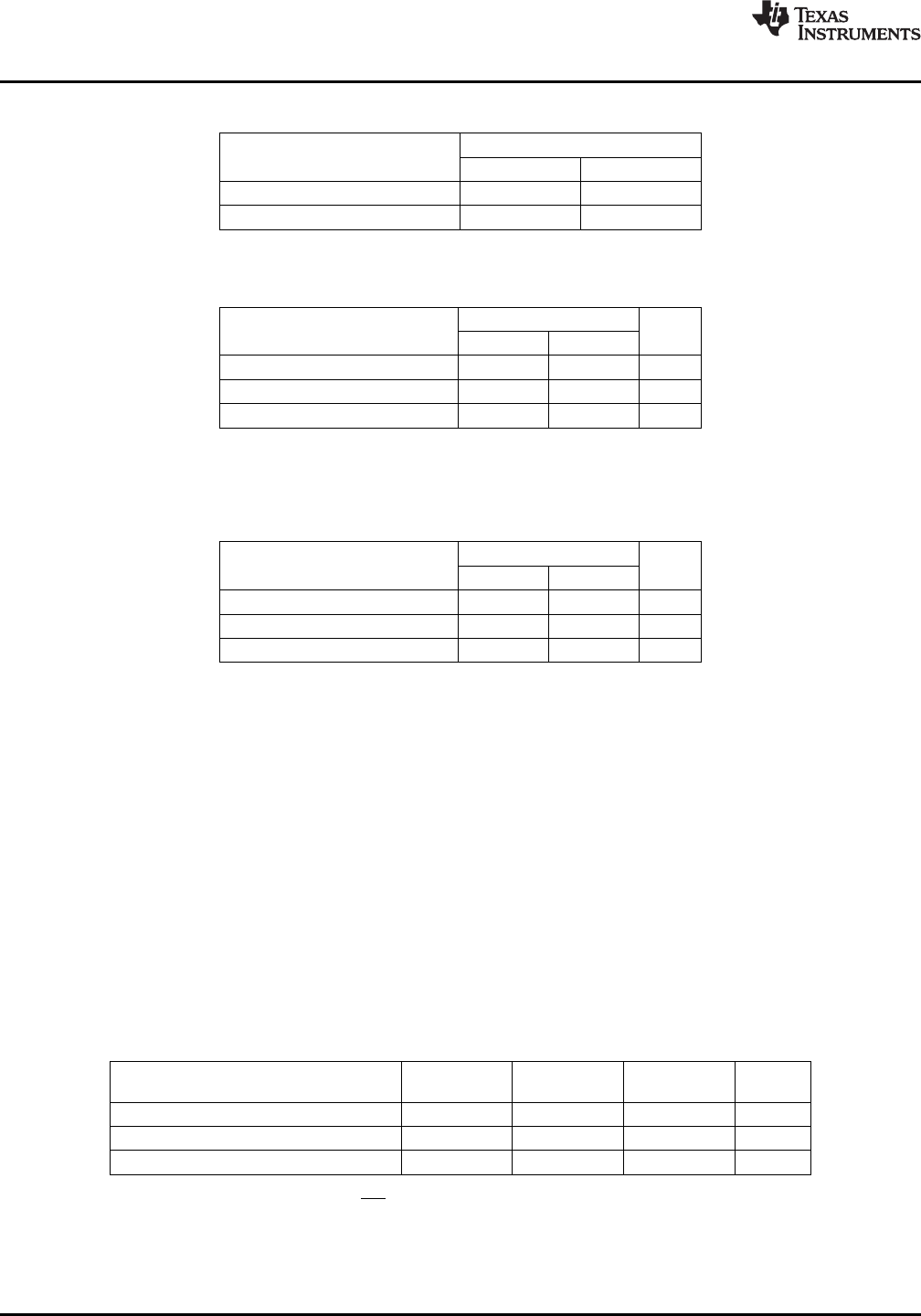
Table 7-7. PLL1 and PLL2 Multiplier Ranges
-1G
PLL MULTIPLIER (PLLM)
MIN MAX
PLL1 Multiplier x14 x32
PLL2 Multiplier x14 x32
Table 7-8. PLLC1 Clock Frequency Ranges
-1G
CLOCK SIGNAL NAME UNIT
MIN MAX
DEV_MXI/DEV_CLKIN
(1)
20 35 MHz
PLLOUT 400 1000 MHz
SYSCLK1 (PLLDIV1 Domain) 1000 MHz
(1) DEV_MXI/DEV_CLKIN input clock is used for both PLL Controllers
(PLLC1 and PLLC2).
Table 7-9. PLLC2 Clock Frequency Ranges
-1G
CLOCK SIGNAL NAME UNIT
MIN MAX
DEV_MXI/DEV_CLKIN
(1)
20 35 MHz
PLLOUT 400 800 MHz
PLL2_SYSCLK1 (to DDR2 PHY) 800 MHz
(1) DEV_MXI/DEV_CLKIN input clock is used for both PLL Controllers
(PLLC1 and PLLC2).
Both PLL1 and PLL2 have stabilization, lock, and reset timing requirements that must be followed.
The PLL stabilization time is the amount of time that must be allotted for the internal PLL regulators to
become stable after the PLL is powered up (after the PLLCTL.PLLPWRDN bit goes through a 1-to-0
transition). The PLL should not be operated until this stabilization time has expired. This stabilization step
must be applied after these resets—a Power-on Reset, a Warm Reset, or a Max Reset, as the
PLLCTL.PLLPWRDN bit resets to a "1". For the PLL stabliziation time value, see Table 7-10.
The PLL reset time is the amount of wait time needed for the PLL to properly reset (writing PLLRST = 1)
before bringing the PLL out of reset (writing PLLRST = 0). For the PLL reset time value, see Table 7-10.
The PLL lock time is the amount of time needed from when the PLL is taken out of reset (PLLRST = 0
with PLLEN = 0) to when to when the PLL controller can be switched to PLL mode (PLLEN = 1). For the
PLL lock time value, see Table 7-10.
Table 7-10. PLL1 and PLL2 Stabilization, Lock, and Reset Times
PLL STABILIZATION/
MIN NOM MAX UNIT
LOCK/RESET TIME
PLL Stabilization Time 150 μs
PLL Lock Time 2000C
(1)
ns
PLL Reset Time 128C
(1)
ns
(1) C = CLKIN cycle time in ns. For example, when DEV_MXI/DEV_CLKIN or AUX_MXI/AUX_CLKIN
frequency is 27 MHz, use C = 37.037 ns.
154 Peripheral Information and Electrical Specifications Copyright © 2009–2012, Texas Instruments Incorporated
Submit Documentation Feedback
Product Folder Link(s): TMS320DM6467T