
Datasheet


Table Of Contents
- 1 Digital Media System-on-Chip (DMSoC)
- Table of Contents
- 2 Revision History
- 3 Device Overview
- 3.1 Device Characteristics
- 3.2 Device Compatibility
- 3.3 ARM Subsystem
- 3.3.1 ARM926EJ-S RISC CPU
- 3.3.2 CP15
- 3.3.3 MMU
- 3.3.4 Caches and Write Buffer
- 3.3.5 Tightly Coupled Memory (TCM)
- 3.3.6 Advanced High-Performance Bus (AHB)
- 3.3.7 Embedded Trace Macrocell (ETM) and Embedded Trace Buffer (ETB)
- 3.3.8 ARM Memory Mapping
- 3.3.9 Peripherals
- 3.3.10 PLL Controller (PLLC)
- 3.3.11 Power and Sleep Controller (PSC)
- 3.3.12 ARM Interrupt Controller (AINTC)
- 3.3.13 System Module
- 3.3.14 Power Management
- 3.4 DSP Subsystem
- 3.5 Memory Map Summary
- 3.6 Pin Assignments
- 3.7 Terminal Functions
- 3.8 Device Support
- 3.9 Documentation Support
- 3.10 Community Resources
- 4 Device Configurations
- 4.1 System Module Registers
- 4.2 Power Considerations
- 4.3 Clock Considerations
- 4.4 Boot Sequence
- 4.5 Configurations At Reset
- 4.6 Configurations After Reset
- 4.7 Multiplexed Pin Configurations
- 4.7.1 Pin Muxing Selection At Reset
- 4.7.2 Pin Muxing Selection After Reset
- 4.7.3 Pin Multiplexing Details
- 4.7.3.1 PCI, HPI, EMIFA, and ATA Pin Muxing
- 4.7.3.2 PWM Signal Muxing
- 4.7.3.3 TSIF0 Input Signal Muxing (Serial/Parallel)
- 4.7.3.4 TSIF0 Output Signal Muxing (Serial/Parallel)
- 4.7.3.5 TSIF1 Input Signal Muxing (Serial Only)
- 4.7.3.6 TSIF1 Output Signal Muxing (Serial Only)
- 4.7.3.7 CRGEN Signal Muxing
- 4.7.3.8 UART0 Pin Muxing
- 4.7.3.9 UART1 Pin Muxing
- 4.7.3.10 UART2 Pin Muxing
- 4.7.3.11 ARM/DSP Communications Interrupts
- 4.7.3.12 Emulation Control
- 4.8 Debugging Considerations
- 5 System Interconnect
- 6 Device Operating Conditions
- 7 Peripheral Information and Electrical Specifications
- 7.1 Parameter Information
- 7.2 Recommended Clock and Control Signal Transition Behavior
- 7.3 Power Supplies
- 7.4 External Clock Input From DEV_MXI/DEV_CLKIN and AUX_MXI/AUX_CLKIN Pins
- 7.5 Clock PLLs
- 7.6 Enhanced Direct Memory Access (EDMA3) Controller
- 7.7 Reset
- 7.8 Interrupts
- 7.9 External Memory Interface (EMIF)
- 7.10 DDR2 Memory Controller
- 7.10.1 DDR2 Memory Controller Electrical Data/Timing
- 7.10.2 DDR2 Interface
- 7.10.2.1 DDR2 Interface Schematic
- 7.10.2.2 Compatible JEDEC DDR2 Devices
- 7.10.2.3 PCB Stackup
- 7.10.2.4 Placement
- 7.10.2.5 DDR2 Keep Out Region
- 7.10.2.6 Bulk Bypass Capacitors
- 7.10.2.7 High-Speed Bypass Capacitors
- 7.10.2.8 Net Classes
- 7.10.2.9 DDR2 Signal Termination
- 7.10.2.10 VREF Routing
- 7.10.2.11 DDR2 CK and ADDR_CTRL Routing
- 7.11 Video Port Interface (VPIF)
- 7.12 Transport Stream Interface (TSIF)
- 7.13 Clock Recovery Generator (CRGEN)
- 7.14 Video Data Conversion Engine (VDCE)
- 7.15 Peripheral Component Interconnect (PCI)
- 7.16 Ethernet MAC (EMAC)
- 7.17 Management Data Input/Output (MDIO)
- 7.18 Host-Port Interface (HPI) Peripheral
- 7.19 USB 2.0 [see Note]
- 7.20 ATA Controller
- 7.21 VLYNQ
- 7.22 Multichannel Audio Serial Port (McASP0/1) Peripherals
- 7.23 Serial Peripheral Interface (SPI)
- 7.24 Universal Asynchronouse Receiver/Transmitter (UART)
- 7.25 Inter-Integrated Circuit (I2C)
- 7.26 Pulse Width Modulator (PWM)
- 7.27 Timers
- 7.28 General-Purpose Input/Output (GPIO)
- 7.29 IEEE 1149.1 JTAG
- 8 Mechanical Packaging and Orderable Information
DM646x
PLL2V
DD18
C2
C1
EMIFilter
+1.8V
0.01 Fμ
PLL2
0.1 Fμ
C4
C3
EMIFilter
+1.8V
0.01 Fμ
PLL1
0.1 Fμ
PLL1V
DD18
TMS320DM6467T
www.ti.com
SPRS605C –JULY 2009–REVISED JUNE 2012
7.5 Clock PLLs
There are two independently controlled PLLs on DM6467T. PLL1 generates the frequencies required for
the ARM, DSP, HDVICP0/1, EDMA, and peripherals. PLL2 generates the frequencies required for the
DDR2 interface. Any input crystal frequency between 27 MHz and 35 MHz can be used for the System
Oscillator (DEV_MXI/DEV_CLKIN). The recommended reference clock for both PLLs is the 33-MHz or
33.3-MHz crystal input. The DM6467T has a third PLL that is embedded within the USB2.0 PHY and the
24-MHz oscillator is its reference clock source. This particular PLL is only usable for USB operation, and is
discussed further in the TMS320DM646x DMSoC Universal Serial Bus (USB) Controller User's Guide
(literature number SPRUER7).
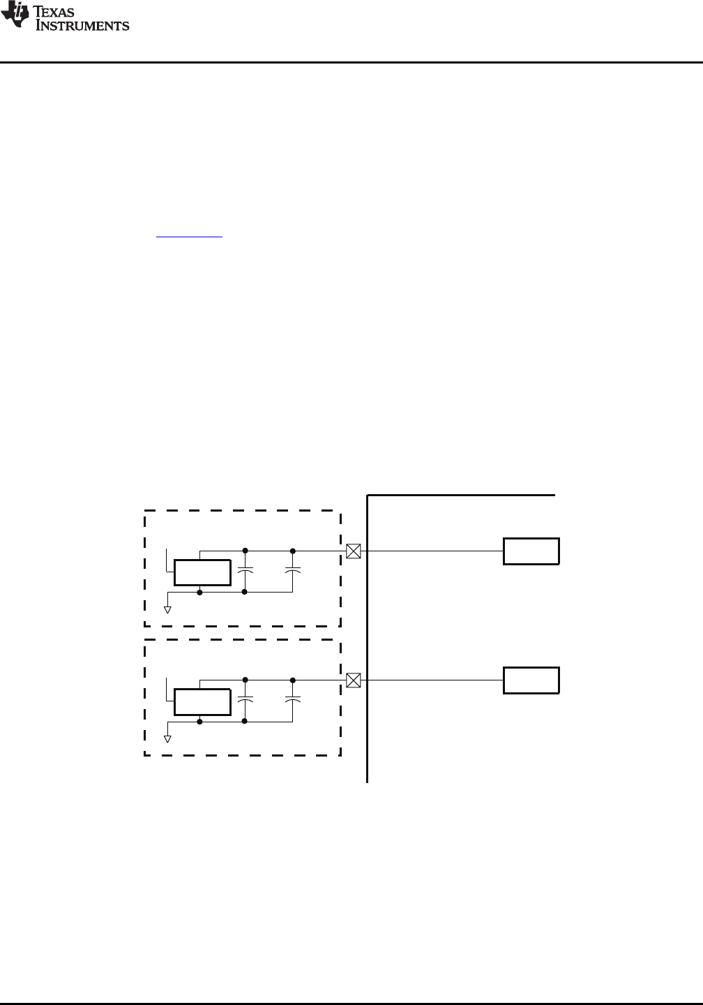
7.5.1 PLL1 and PLL2
Both PLL1 and PLL2 power are supplied externally via the 1.8-V PLL power-supply pins (PLL1V
DD18
and
PLL2V
DD18
). An external EMI filter circuit must be added to PLL1V
DD18
and PLL2V
DD18
, as shown in
Figure 7-11. The 1.8-V supply of the EMI filters must be from the same 1.8-V power plane supplying the
device’s 1.8-V I/O power-supply pins (DV
DDR2
). TI recommends EMI filter manufacturer Murata, part
number NFM18CC222R1C3.
All PLL external components (C1, C2, C3, C4, and the EMI Filters) must be placed as close to the device
as possible. For the best performance, TI recommends that all the PLL external components be on a
single side of the board without jumpers, switches, or components other than the ones shown in Figure 7-
11. For reduced PLL jitter, maximize the spacing between switching signals and the PLL external
components (C1, C2, C3, C4, and the EMI Filters).
Figure 7-11. PLL1 and PLL2 External Connection
The minimum CLKIN rise and fall times should also be observed. For the input clock timing requirements,
see Section 7.5.5, Clock PLL Electrical Data/Timing (Input and Output Clocks).
There is an allowable range for PLL multiplier (PLLM). There is a minimum and maximum operating
frequency for DEV_MXI/DEV_CLKIN, PLLOUT, AUX_MXI/AUX_CLKIN, and the device clocks
(SYSCLKs). The PLL Controllers must be configured not to exceed any of these constraints documented
in this section (certain combinations of external clock inputs, internal dividers, and PLL multiply ratios
might not be supported). For these constraints (ranges), see Table 7-7 through Table 7-9 .
Copyright © 2009–2012, Texas Instruments Incorporated Peripheral Information and Electrical Specifications 153
Submit Documentation Feedback
Product Folder Link(s): TMS320DM6467T