
Datasheet


Table Of Contents
- 1 Digital Media System-on-Chip (DMSoC)
- Table of Contents
- 2 Revision History
- 3 Device Overview
- 3.1 Device Characteristics
- 3.2 Device Compatibility
- 3.3 ARM Subsystem
- 3.3.1 ARM926EJ-S RISC CPU
- 3.3.2 CP15
- 3.3.3 MMU
- 3.3.4 Caches and Write Buffer
- 3.3.5 Tightly Coupled Memory (TCM)
- 3.3.6 Advanced High-Performance Bus (AHB)
- 3.3.7 Embedded Trace Macrocell (ETM) and Embedded Trace Buffer (ETB)
- 3.3.8 ARM Memory Mapping
- 3.3.9 Peripherals
- 3.3.10 PLL Controller (PLLC)
- 3.3.11 Power and Sleep Controller (PSC)
- 3.3.12 ARM Interrupt Controller (AINTC)
- 3.3.13 System Module
- 3.3.14 Power Management
- 3.4 DSP Subsystem
- 3.5 Memory Map Summary
- 3.6 Pin Assignments
- 3.7 Terminal Functions
- 3.8 Device Support
- 3.9 Documentation Support
- 3.10 Community Resources
- 4 Device Configurations
- 4.1 System Module Registers
- 4.2 Power Considerations
- 4.3 Clock Considerations
- 4.4 Boot Sequence
- 4.5 Configurations At Reset
- 4.6 Configurations After Reset
- 4.7 Multiplexed Pin Configurations
- 4.7.1 Pin Muxing Selection At Reset
- 4.7.2 Pin Muxing Selection After Reset
- 4.7.3 Pin Multiplexing Details
- 4.7.3.1 PCI, HPI, EMIFA, and ATA Pin Muxing
- 4.7.3.2 PWM Signal Muxing
- 4.7.3.3 TSIF0 Input Signal Muxing (Serial/Parallel)
- 4.7.3.4 TSIF0 Output Signal Muxing (Serial/Parallel)
- 4.7.3.5 TSIF1 Input Signal Muxing (Serial Only)
- 4.7.3.6 TSIF1 Output Signal Muxing (Serial Only)
- 4.7.3.7 CRGEN Signal Muxing
- 4.7.3.8 UART0 Pin Muxing
- 4.7.3.9 UART1 Pin Muxing
- 4.7.3.10 UART2 Pin Muxing
- 4.7.3.11 ARM/DSP Communications Interrupts
- 4.7.3.12 Emulation Control
- 4.8 Debugging Considerations
- 5 System Interconnect
- 6 Device Operating Conditions
- 7 Peripheral Information and Electrical Specifications
- 7.1 Parameter Information
- 7.2 Recommended Clock and Control Signal Transition Behavior
- 7.3 Power Supplies
- 7.4 External Clock Input From DEV_MXI/DEV_CLKIN and AUX_MXI/AUX_CLKIN Pins
- 7.5 Clock PLLs
- 7.6 Enhanced Direct Memory Access (EDMA3) Controller
- 7.7 Reset
- 7.8 Interrupts
- 7.9 External Memory Interface (EMIF)
- 7.10 DDR2 Memory Controller
- 7.10.1 DDR2 Memory Controller Electrical Data/Timing
- 7.10.2 DDR2 Interface
- 7.10.2.1 DDR2 Interface Schematic
- 7.10.2.2 Compatible JEDEC DDR2 Devices
- 7.10.2.3 PCB Stackup
- 7.10.2.4 Placement
- 7.10.2.5 DDR2 Keep Out Region
- 7.10.2.6 Bulk Bypass Capacitors
- 7.10.2.7 High-Speed Bypass Capacitors
- 7.10.2.8 Net Classes
- 7.10.2.9 DDR2 Signal Termination
- 7.10.2.10 VREF Routing
- 7.10.2.11 DDR2 CK and ADDR_CTRL Routing
- 7.11 Video Port Interface (VPIF)
- 7.12 Transport Stream Interface (TSIF)
- 7.13 Clock Recovery Generator (CRGEN)
- 7.14 Video Data Conversion Engine (VDCE)
- 7.15 Peripheral Component Interconnect (PCI)
- 7.16 Ethernet MAC (EMAC)
- 7.17 Management Data Input/Output (MDIO)
- 7.18 Host-Port Interface (HPI) Peripheral
- 7.19 USB 2.0 [see Note]
- 7.20 ATA Controller
- 7.21 VLYNQ
- 7.22 Multichannel Audio Serial Port (McASP0/1) Peripherals
- 7.23 Serial Peripheral Interface (SPI)
- 7.24 Universal Asynchronouse Receiver/Transmitter (UART)
- 7.25 Inter-Integrated Circuit (I2C)
- 7.26 Pulse Width Modulator (PWM)
- 7.27 Timers
- 7.28 General-Purpose Input/Output (GPIO)
- 7.29 IEEE 1149.1 JTAG
- 8 Mechanical Packaging and Orderable Information
( )
C C
1 2
C
L
C C
1 2
=
+
DEV_MXI/
DEV_CLKIN
DEV_MXO
C1 C2
Crystal
DEV_V
SS
33.3 MHz
1.8 V
DEV_DV
DD18
1.3 V
DEV_CV
DD
DEV_DV
SS
TMS320DM6467T
www.ti.com
SPRS605C –JULY 2009–REVISED JUNE 2012
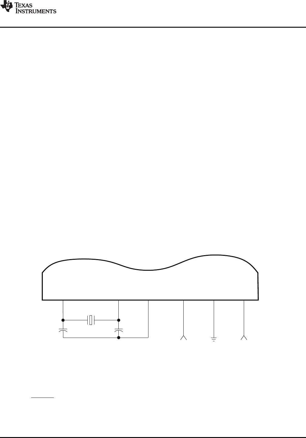
7.4 External Clock Input From DEV_MXI/DEV_CLKIN and AUX_MXI/AUX_CLKIN Pins
The DM6467T device includes two options to provide an external clock input for both the system and
auxiliary oscillators:
• Use an on-chip oscillator with external crystal (fundamental parallel resonant mode only, no overtone
support).
• Use an external 1.8-V LVCMOS-compatible clock input.
Any input crystal frequency between 27 MHz and 35 MHz can be used for the System Oscillator
(DEV_MXI/DEV_CLKIN).
The optimal external clock input frequency for the crystals are 33 MHz or 33.3 MHz for the system
oscillator (DEV_MXI/DEV_CLKIN) and 24 MHz for the auxiliary oscillator. Section 7.4.1.1 provides more
details on Option 1, using an on-chip oscillator with external crystal for the 33.3-MHz system oscillator.
Section 7.4.1.2 provides more details on Option 1, using an on-chip oscillator with external crystal for the
24-MHz auxiliary oscillator. Section 7.4.2.1 provides details on Option 2, using an external 1.8-V
LVCMOS-compatible clock input for the 33.3-MHz system oscillator. Section 7.4.2 provides details on
Option 2, using an external 1.8-V LVCMOS-compatible clock input for the 24-MHz auxiliary oscillator.
7.4.1 Clock Input Option 1—Crystal
7.4.1.1 33.3-MHz for System Oscillator Clock Input Option 1—Crystal
In this option, a crystal is used as the external clock input to the DM6467T system oscillator.
The 33.3-MHz oscillator provides the reference clock for all DM6467T subsystems and peripherals. The
on-chip oscillator requires an external 33.3-MHz crystal connected across the DEV_MXI and DEV_MXO
pins, along with two load capacitors, as shown in Figure 7-7. The external crystal load capacitors must be
connected only to the 33.3-MHz oscillator ground pin (DEV_V
SS
). Do not connect to board ground (V
SS
).
The DEV_DV
DD18
pin can be connected to the same 1.8 V power supply as DV
DDR2
.
Figure 7-7. 33.3-MHz System Oscillator
The load capacitors, C1 and C2, should be chosen such that the equation is satisfied (for typical values,
see Table 7-5). C
L
in the equation is the load specified by the crystal manufacturer. All discrete
components used to implement the oscillator circuit should be placed as close as possible to the
associated oscillator pins (DEV_MXI and DEV_MXO) and to the DEV_V
SS
pin.
Copyright © 2009–2012, Texas Instruments Incorporated Peripheral Information and Electrical Specifications 149
Submit Documentation Feedback
Product Folder Link(s): TMS320DM6467T