
Datasheet


Table Of Contents
- 1 Digital Media System-on-Chip (DMSoC)
- Table of Contents
- 2 Revision History
- 3 Device Overview
- 3.1 Device Characteristics
- 3.2 Device Compatibility
- 3.3 ARM Subsystem
- 3.3.1 ARM926EJ-S RISC CPU
- 3.3.2 CP15
- 3.3.3 MMU
- 3.3.4 Caches and Write Buffer
- 3.3.5 Tightly Coupled Memory (TCM)
- 3.3.6 Advanced High-Performance Bus (AHB)
- 3.3.7 Embedded Trace Macrocell (ETM) and Embedded Trace Buffer (ETB)
- 3.3.8 ARM Memory Mapping
- 3.3.9 Peripherals
- 3.3.10 PLL Controller (PLLC)
- 3.3.11 Power and Sleep Controller (PSC)
- 3.3.12 ARM Interrupt Controller (AINTC)
- 3.3.13 System Module
- 3.3.14 Power Management
- 3.4 DSP Subsystem
- 3.5 Memory Map Summary
- 3.6 Pin Assignments
- 3.7 Terminal Functions
- 3.8 Device Support
- 3.9 Documentation Support
- 3.10 Community Resources
- 4 Device Configurations
- 4.1 System Module Registers
- 4.2 Power Considerations
- 4.3 Clock Considerations
- 4.4 Boot Sequence
- 4.5 Configurations At Reset
- 4.6 Configurations After Reset
- 4.7 Multiplexed Pin Configurations
- 4.7.1 Pin Muxing Selection At Reset
- 4.7.2 Pin Muxing Selection After Reset
- 4.7.3 Pin Multiplexing Details
- 4.7.3.1 PCI, HPI, EMIFA, and ATA Pin Muxing
- 4.7.3.2 PWM Signal Muxing
- 4.7.3.3 TSIF0 Input Signal Muxing (Serial/Parallel)
- 4.7.3.4 TSIF0 Output Signal Muxing (Serial/Parallel)
- 4.7.3.5 TSIF1 Input Signal Muxing (Serial Only)
- 4.7.3.6 TSIF1 Output Signal Muxing (Serial Only)
- 4.7.3.7 CRGEN Signal Muxing
- 4.7.3.8 UART0 Pin Muxing
- 4.7.3.9 UART1 Pin Muxing
- 4.7.3.10 UART2 Pin Muxing
- 4.7.3.11 ARM/DSP Communications Interrupts
- 4.7.3.12 Emulation Control
- 4.8 Debugging Considerations
- 5 System Interconnect
- 6 Device Operating Conditions
- 7 Peripheral Information and Electrical Specifications
- 7.1 Parameter Information
- 7.2 Recommended Clock and Control Signal Transition Behavior
- 7.3 Power Supplies
- 7.4 External Clock Input From DEV_MXI/DEV_CLKIN and AUX_MXI/AUX_CLKIN Pins
- 7.5 Clock PLLs
- 7.6 Enhanced Direct Memory Access (EDMA3) Controller
- 7.7 Reset
- 7.8 Interrupts
- 7.9 External Memory Interface (EMIF)
- 7.10 DDR2 Memory Controller
- 7.10.1 DDR2 Memory Controller Electrical Data/Timing
- 7.10.2 DDR2 Interface
- 7.10.2.1 DDR2 Interface Schematic
- 7.10.2.2 Compatible JEDEC DDR2 Devices
- 7.10.2.3 PCB Stackup
- 7.10.2.4 Placement
- 7.10.2.5 DDR2 Keep Out Region
- 7.10.2.6 Bulk Bypass Capacitors
- 7.10.2.7 High-Speed Bypass Capacitors
- 7.10.2.8 Net Classes
- 7.10.2.9 DDR2 Signal Termination
- 7.10.2.10 VREF Routing
- 7.10.2.11 DDR2 CK and ADDR_CTRL Routing
- 7.11 Video Port Interface (VPIF)
- 7.12 Transport Stream Interface (TSIF)
- 7.13 Clock Recovery Generator (CRGEN)
- 7.14 Video Data Conversion Engine (VDCE)
- 7.15 Peripheral Component Interconnect (PCI)
- 7.16 Ethernet MAC (EMAC)
- 7.17 Management Data Input/Output (MDIO)
- 7.18 Host-Port Interface (HPI) Peripheral
- 7.19 USB 2.0 [see Note]
- 7.20 ATA Controller
- 7.21 VLYNQ
- 7.22 Multichannel Audio Serial Port (McASP0/1) Peripherals
- 7.23 Serial Peripheral Interface (SPI)
- 7.24 Universal Asynchronouse Receiver/Transmitter (UART)
- 7.25 Inter-Integrated Circuit (I2C)
- 7.26 Pulse Width Modulator (PWM)
- 7.27 Timers
- 7.28 General-Purpose Input/Output (GPIO)
- 7.29 IEEE 1149.1 JTAG
- 8 Mechanical Packaging and Orderable Information
TMS320DM6467T
SPRS605C –JULY 2009–REVISED JUNE 2012
www.ti.com
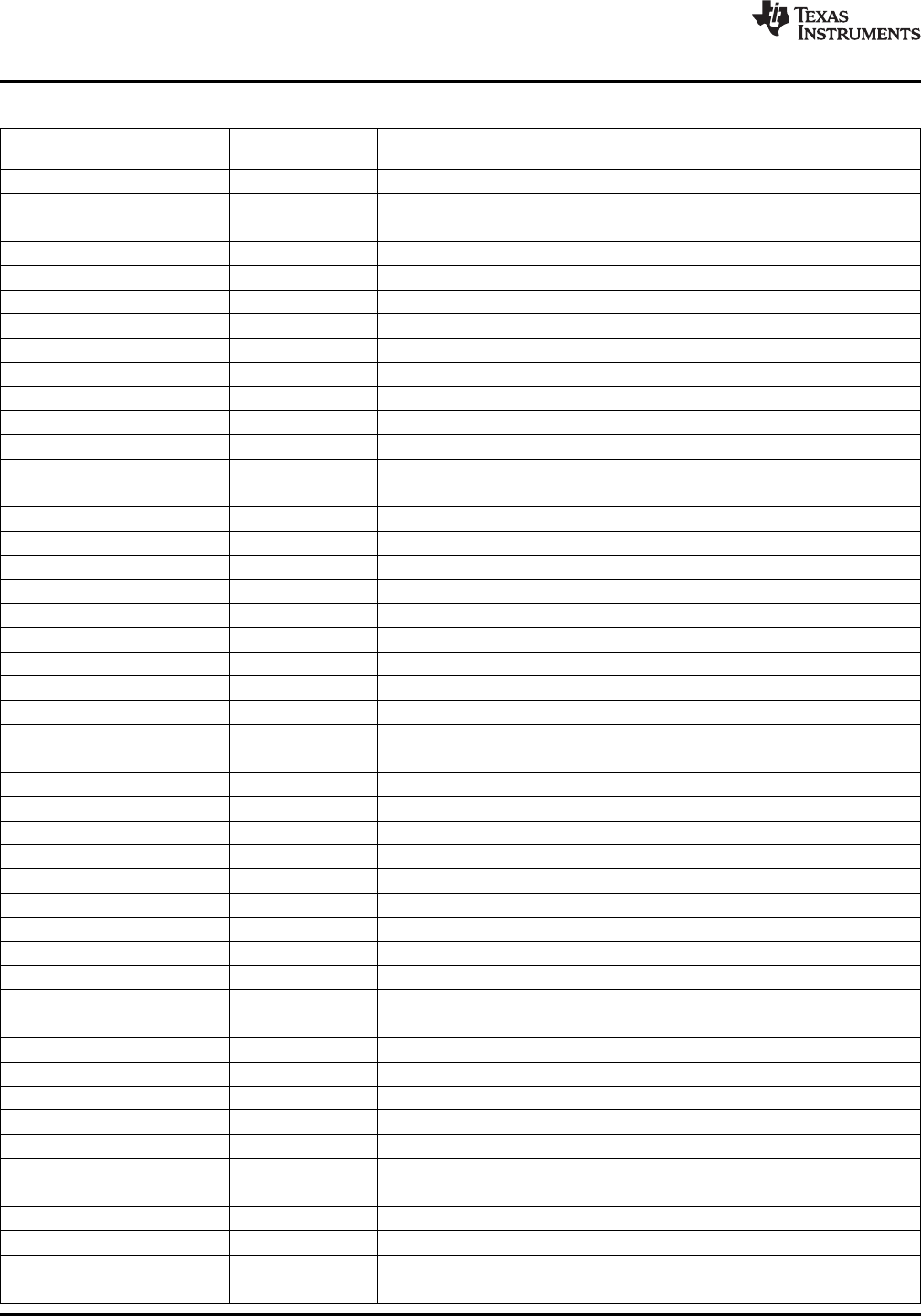
Table 7-4. PSC Registers
REGISTER
HEX ADDRESS RANGE DESCRIPTION
ACRONYM
0x01C4 1000 PID Peripheral Revision and Class Information Register
0x01C4 1004 - 0x01C4 1017 – Reserved
0x01C4 1018 INTEVAL Interrupt Evaluation Register
0x01C4 101C - 0x01C4 1039 – Reserved
0x01C4 1040 MERRPR0 Module Error Pending 0 (mod 0- 31) Register
0x01C4 1044 MERRPR1 Module Error Pending 1 (mod 32- 63) Register
0x01C4 1048 - 0x01C4 1049 – Reserved
0x01C4 1050 MERRCR0 Module Error Clear 0 (mod 0 - 31) Register
0x01C4 1054 MERRCR1 Module Error Clear 1 (mod 32 - 63) Register
0x01C4 1058 - 0x01C4 111F Reserved
0x01C4 1120 PTCMD Power Domain Transition Command Register
0x01C4 1124 - 0x01C4 1127 – Reserved
0x01C4 1128 PTSTAT Power Domain Transition Status Register
0x01C4 112C - 0x01C4 11FF – Reserved
0x01C4 1200 PDSTAT0 Power Domain Status 0 Register (Always On)
0x01C4 1204 - 0x01C4 12FF – Reserved
0x01C4 1300 PDCTL0 Power Domain Control 0 Register (Always On)
0x01C4 1304 - 0x01C4 17FF – Reserved
0x01C4 1800 - 0x01C4 1803 – Reserved
0x01C4 1804 MDSTAT1 Module Status 1 Register (C64x+ CPU)
0x01C4 1808 MDSTAT2 Module Status 2 Register (HDVICP0)
0x01C4 180C MDSTAT3 Module Status 3 Register (HDVICP1)
0x01C4 1810 MDSTAT4 Module Status 4 Register (EDMA CC)
0x01C4 1814 MDSTAT5 Module Status 5 Register (EDMA TC0)
0x01C4 1818 MDSTAT6 Module Status 6 Register (EDMA TC1)
0x01C4 181C MDSTAT7 Module Status 7 Register (EDMA TC2)
0x01C4 1820 MDSTAT8 Module Status 8 Register (EDMA TC3)
0x01C4 1824 MDSTAT9 Module Status 9 Register (USB)
0x01C4 1828 MDSTAT10 Module Status 10 Register (ATA)
0x01C4 182C MDSTAT11 Module Status 11 Register (VLYNQ)
0x01C4 1830 MDSTAT12 Module Status 12 Register (HPI)
0x01C4 1834 MDSTAT13 Module Status 13 Register (PCI)
0x01C4 1838 MDSTAT14 Module Status 14 Register (EMAC)
0x01C4 183C MDSTAT15 Module Status 15 Register (VDCE)
0x01C4 1840 MDSTAT16 Module Status 16 Register (Vdieo Port)
0x01C4 1844 MDSTAT17 Module Status 17 Register (Video Port)
0x01C4 1848 MDSTAT18 Module Status 18 Register (TSIF0)
0x01C4 184C MDSTAT19 Module Status 19 Register (TSIF1)
0x01C4 1850 MDSTAT20 Module Status 20 Register (DDR2 Mem Ctlr)
0x01C4 1854 MDSTAT21 Module Status 21 Register (EMIFA)
0x01C4 1858 MDSTAT22 Module Status 22 Register (McASP0)
0x01C4 185C MDSTAT23 Module Status 23 Register (McASP1)
0x01C4 1860 MDSTAT24 Module Status 24 Register (CRGEN0)
0x01C4 1864 MDSTAT25 Module Status 25 Register (CRGEN1)
0x01C4 1868 MDSTAT26 Module Status 26 Register (UART0)
0x01C4 186C MDSTAT27 Module Status 27 Register (UART1)
0x01C4 1870 MDSTAT28 Module Status 28 Register (UART2)
146 Peripheral Information and Electrical Specifications Copyright © 2009–2012, Texas Instruments Incorporated
Submit Documentation Feedback
Product Folder Link(s): TMS320DM6467T