
Datasheet


Table Of Contents
- 1 Digital Media System-on-Chip (DMSoC)
- Table of Contents
- 2 Revision History
- 3 Device Overview
- 3.1 Device Characteristics
- 3.2 Device Compatibility
- 3.3 ARM Subsystem
- 3.3.1 ARM926EJ-S RISC CPU
- 3.3.2 CP15
- 3.3.3 MMU
- 3.3.4 Caches and Write Buffer
- 3.3.5 Tightly Coupled Memory (TCM)
- 3.3.6 Advanced High-Performance Bus (AHB)
- 3.3.7 Embedded Trace Macrocell (ETM) and Embedded Trace Buffer (ETB)
- 3.3.8 ARM Memory Mapping
- 3.3.9 Peripherals
- 3.3.10 PLL Controller (PLLC)
- 3.3.11 Power and Sleep Controller (PSC)
- 3.3.12 ARM Interrupt Controller (AINTC)
- 3.3.13 System Module
- 3.3.14 Power Management
- 3.4 DSP Subsystem
- 3.5 Memory Map Summary
- 3.6 Pin Assignments
- 3.7 Terminal Functions
- 3.8 Device Support
- 3.9 Documentation Support
- 3.10 Community Resources
- 4 Device Configurations
- 4.1 System Module Registers
- 4.2 Power Considerations
- 4.3 Clock Considerations
- 4.4 Boot Sequence
- 4.5 Configurations At Reset
- 4.6 Configurations After Reset
- 4.7 Multiplexed Pin Configurations
- 4.7.1 Pin Muxing Selection At Reset
- 4.7.2 Pin Muxing Selection After Reset
- 4.7.3 Pin Multiplexing Details
- 4.7.3.1 PCI, HPI, EMIFA, and ATA Pin Muxing
- 4.7.3.2 PWM Signal Muxing
- 4.7.3.3 TSIF0 Input Signal Muxing (Serial/Parallel)
- 4.7.3.4 TSIF0 Output Signal Muxing (Serial/Parallel)
- 4.7.3.5 TSIF1 Input Signal Muxing (Serial Only)
- 4.7.3.6 TSIF1 Output Signal Muxing (Serial Only)
- 4.7.3.7 CRGEN Signal Muxing
- 4.7.3.8 UART0 Pin Muxing
- 4.7.3.9 UART1 Pin Muxing
- 4.7.3.10 UART2 Pin Muxing
- 4.7.3.11 ARM/DSP Communications Interrupts
- 4.7.3.12 Emulation Control
- 4.8 Debugging Considerations
- 5 System Interconnect
- 6 Device Operating Conditions
- 7 Peripheral Information and Electrical Specifications
- 7.1 Parameter Information
- 7.2 Recommended Clock and Control Signal Transition Behavior
- 7.3 Power Supplies
- 7.4 External Clock Input From DEV_MXI/DEV_CLKIN and AUX_MXI/AUX_CLKIN Pins
- 7.5 Clock PLLs
- 7.6 Enhanced Direct Memory Access (EDMA3) Controller
- 7.7 Reset
- 7.8 Interrupts
- 7.9 External Memory Interface (EMIF)
- 7.10 DDR2 Memory Controller
- 7.10.1 DDR2 Memory Controller Electrical Data/Timing
- 7.10.2 DDR2 Interface
- 7.10.2.1 DDR2 Interface Schematic
- 7.10.2.2 Compatible JEDEC DDR2 Devices
- 7.10.2.3 PCB Stackup
- 7.10.2.4 Placement
- 7.10.2.5 DDR2 Keep Out Region
- 7.10.2.6 Bulk Bypass Capacitors
- 7.10.2.7 High-Speed Bypass Capacitors
- 7.10.2.8 Net Classes
- 7.10.2.9 DDR2 Signal Termination
- 7.10.2.10 VREF Routing
- 7.10.2.11 DDR2 CK and ADDR_CTRL Routing
- 7.11 Video Port Interface (VPIF)
- 7.12 Transport Stream Interface (TSIF)
- 7.13 Clock Recovery Generator (CRGEN)
- 7.14 Video Data Conversion Engine (VDCE)
- 7.15 Peripheral Component Interconnect (PCI)
- 7.16 Ethernet MAC (EMAC)
- 7.17 Management Data Input/Output (MDIO)
- 7.18 Host-Port Interface (HPI) Peripheral
- 7.19 USB 2.0 [see Note]
- 7.20 ATA Controller
- 7.21 VLYNQ
- 7.22 Multichannel Audio Serial Port (McASP0/1) Peripherals
- 7.23 Serial Peripheral Interface (SPI)
- 7.24 Universal Asynchronouse Receiver/Transmitter (UART)
- 7.25 Inter-Integrated Circuit (I2C)
- 7.26 Pulse Width Modulator (PWM)
- 7.27 Timers
- 7.28 General-Purpose Input/Output (GPIO)
- 7.29 IEEE 1149.1 JTAG
- 8 Mechanical Packaging and Orderable Information
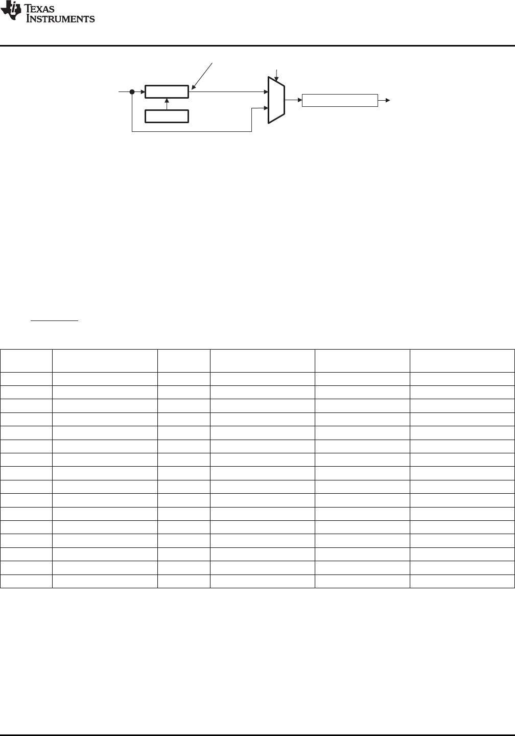
PLLDIV1(/1Prog)
PLL2_SYSCLK1
(DDR2_PHY)
1
0
PLLEN
PLL
PLLM
CLKIN/OSCIN
(A)
(A) AsselectedbythePLL2PLLCTL register
PLLOUT
TMS320DM6467T
www.ti.com
SPRS605C –JULY 2009–REVISED JUNE 2012
Figure 7-6. PLL2 Structure Block Diagram
7.3.5 Power and Sleep Controller (PSC)
The Power and Sleep Controller (PSC) controls device power by gating off clocks to individual
peripherals/modules. The PSC consists of a Global PSC (GPSC) and a set of Local PSCs (LPSCs). The
GPSC contains memory mapped registers, PSC interrupt control, and a state machine for each
peripheral/module. An LPSC is associated with each peripheral/module and provides clock and reset
control. The GPSC controls all of the DM6467T's LPSCs. The ARM Subsystem does not have an LPSC
module. ARM sleep mode is accomplished through the wait for interrupt instruction. The LPSCs for
DM6467T are shown in Table 7-3. The PSC Register memory map is given in Table 7-4. For more details
on the PSC, see the TMS320DM646x DMSoC ARM Subsystem Reference Guide (literature number
SPRUEP9).
Table 7-3. DM6467T LPSC Assignments
LPSC PERIPHERAL/MODULE LPSC PERIPHERAL/MODULE LPSC PERIPHERAL/MODULE
NUMBER NUMBER NUMBER
0 Reserved 16 Video Port 32 SPI
1 C64x+ CPU 17 Video Port 33 GPIO
2 HDVICP0 18 TSIF0 34 TIMER0
3 HDVICP1 19 TSIF1 35 TIMER1
4 EDMA CC 20 DDR2 Memory Controller 36 Reserved
5 EDMA TC0 21 EMIFA 37 Reserved
6 EDMA TC1 22 McASP0 38 Reserved
7 EDMA TC2 23 McASP1 39 Reserved
8 EDMA TC3 24 CRGEN0 40 Reserved
9 USB2.0 25 CRGEN1 41 Reserved
10 ATA 26 UART0 42 Reserved
11 VLYNQ 27 UART1 43 Reserved
12 HPI 28 UART2 44 Reserved
13 PCI 29 PWM0 45 ARM INTC
14 EMAC/MDIO 30 PWM1
15 VDCE 31 I2C
Copyright © 2009–2012, Texas Instruments Incorporated Peripheral Information and Electrical Specifications 145
Submit Documentation Feedback
Product Folder Link(s): TMS320DM6467T