
Datasheet


Table Of Contents
- 1 Digital Media System-on-Chip (DMSoC)
- Table of Contents
- 2 Revision History
- 3 Device Overview
- 3.1 Device Characteristics
- 3.2 Device Compatibility
- 3.3 ARM Subsystem
- 3.3.1 ARM926EJ-S RISC CPU
- 3.3.2 CP15
- 3.3.3 MMU
- 3.3.4 Caches and Write Buffer
- 3.3.5 Tightly Coupled Memory (TCM)
- 3.3.6 Advanced High-Performance Bus (AHB)
- 3.3.7 Embedded Trace Macrocell (ETM) and Embedded Trace Buffer (ETB)
- 3.3.8 ARM Memory Mapping
- 3.3.9 Peripherals
- 3.3.10 PLL Controller (PLLC)
- 3.3.11 Power and Sleep Controller (PSC)
- 3.3.12 ARM Interrupt Controller (AINTC)
- 3.3.13 System Module
- 3.3.14 Power Management
- 3.4 DSP Subsystem
- 3.5 Memory Map Summary
- 3.6 Pin Assignments
- 3.7 Terminal Functions
- 3.8 Device Support
- 3.9 Documentation Support
- 3.10 Community Resources
- 4 Device Configurations
- 4.1 System Module Registers
- 4.2 Power Considerations
- 4.3 Clock Considerations
- 4.4 Boot Sequence
- 4.5 Configurations At Reset
- 4.6 Configurations After Reset
- 4.7 Multiplexed Pin Configurations
- 4.7.1 Pin Muxing Selection At Reset
- 4.7.2 Pin Muxing Selection After Reset
- 4.7.3 Pin Multiplexing Details
- 4.7.3.1 PCI, HPI, EMIFA, and ATA Pin Muxing
- 4.7.3.2 PWM Signal Muxing
- 4.7.3.3 TSIF0 Input Signal Muxing (Serial/Parallel)
- 4.7.3.4 TSIF0 Output Signal Muxing (Serial/Parallel)
- 4.7.3.5 TSIF1 Input Signal Muxing (Serial Only)
- 4.7.3.6 TSIF1 Output Signal Muxing (Serial Only)
- 4.7.3.7 CRGEN Signal Muxing
- 4.7.3.8 UART0 Pin Muxing
- 4.7.3.9 UART1 Pin Muxing
- 4.7.3.10 UART2 Pin Muxing
- 4.7.3.11 ARM/DSP Communications Interrupts
- 4.7.3.12 Emulation Control
- 4.8 Debugging Considerations
- 5 System Interconnect
- 6 Device Operating Conditions
- 7 Peripheral Information and Electrical Specifications
- 7.1 Parameter Information
- 7.2 Recommended Clock and Control Signal Transition Behavior
- 7.3 Power Supplies
- 7.4 External Clock Input From DEV_MXI/DEV_CLKIN and AUX_MXI/AUX_CLKIN Pins
- 7.5 Clock PLLs
- 7.6 Enhanced Direct Memory Access (EDMA3) Controller
- 7.7 Reset
- 7.8 Interrupts
- 7.9 External Memory Interface (EMIF)
- 7.10 DDR2 Memory Controller
- 7.10.1 DDR2 Memory Controller Electrical Data/Timing
- 7.10.2 DDR2 Interface
- 7.10.2.1 DDR2 Interface Schematic
- 7.10.2.2 Compatible JEDEC DDR2 Devices
- 7.10.2.3 PCB Stackup
- 7.10.2.4 Placement
- 7.10.2.5 DDR2 Keep Out Region
- 7.10.2.6 Bulk Bypass Capacitors
- 7.10.2.7 High-Speed Bypass Capacitors
- 7.10.2.8 Net Classes
- 7.10.2.9 DDR2 Signal Termination
- 7.10.2.10 VREF Routing
- 7.10.2.11 DDR2 CK and ADDR_CTRL Routing
- 7.11 Video Port Interface (VPIF)
- 7.12 Transport Stream Interface (TSIF)
- 7.13 Clock Recovery Generator (CRGEN)
- 7.14 Video Data Conversion Engine (VDCE)
- 7.15 Peripheral Component Interconnect (PCI)
- 7.16 Ethernet MAC (EMAC)
- 7.17 Management Data Input/Output (MDIO)
- 7.18 Host-Port Interface (HPI) Peripheral
- 7.19 USB 2.0 [see Note]
- 7.20 ATA Controller
- 7.21 VLYNQ
- 7.22 Multichannel Audio Serial Port (McASP0/1) Peripherals
- 7.23 Serial Peripheral Interface (SPI)
- 7.24 Universal Asynchronouse Receiver/Transmitter (UART)
- 7.25 Inter-Integrated Circuit (I2C)
- 7.26 Pulse Width Modulator (PWM)
- 7.27 Timers
- 7.28 General-Purpose Input/Output (GPIO)
- 7.29 IEEE 1149.1 JTAG
- 8 Mechanical Packaging and Orderable Information
TMS320DM6467T
www.ti.com
SPRS605C –JULY 2009–REVISED JUNE 2012
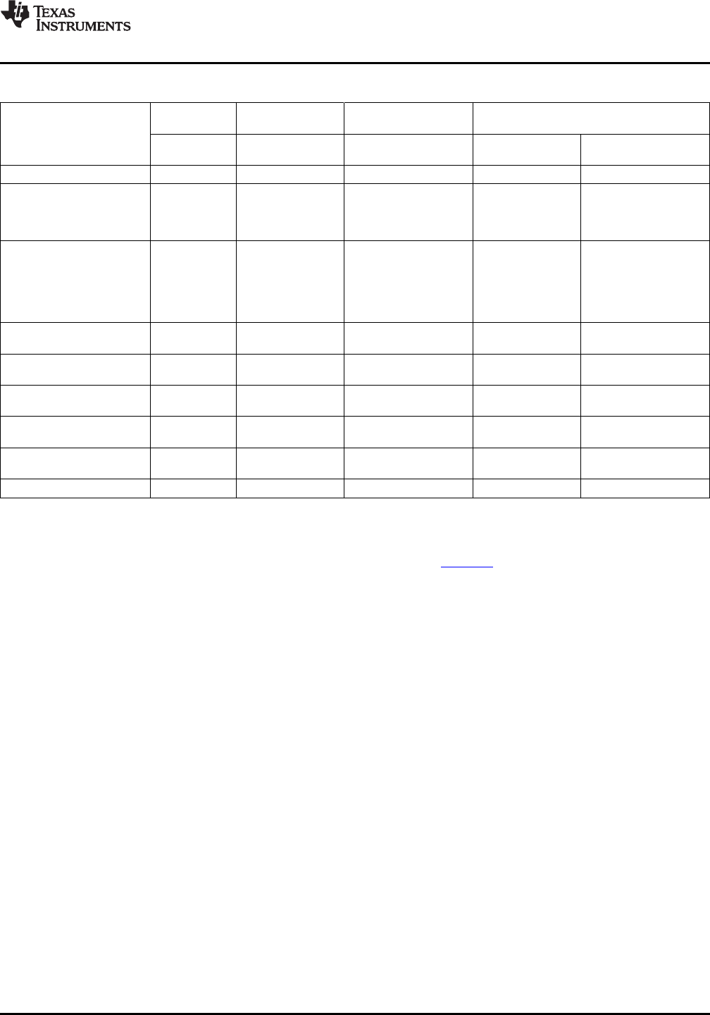
Table 7-2. DM6467T Clock Domains
CLOCK DOMAIN CLOCK FIXED RATIO vs.
CLOCK MODES FREQUENCY (MHz)
DOMAIN SOURCE SYSCLK1 FREQ
SUBSYSTEM
BYPASS MODE
PLL MODE (-1G)
(1)
[default RATIO]
DSP Subsystem PLLDIV1 PLLC1 SYSCLK1 1:1 33.30 MHz 999 MHz
ARM926 Subsystem, 1:2
EDMA3, HDVICP, PCI,
PLLDIV2 PLLC1 SYSCLK2 16.65 MHz 499.50 MHz
VDCE, VPIF, TSIFs, DDR2
Mem Ctlr
Peripherals (GPIO, Timers, 1:4
I2C, PWMs, HPI, EMAC,
EMIFA, VLYNQ, SPI, ARM
PLLDIV3 PLLC1 SYSCLK3 8.33 MHz 249.75 MHz
INTC, USB2.0, UARTs,
McASPs, CRGENs,
SYSTEM)
ATA 1:6 [default]
PLLDIV4 PLLC1 SYSCLK4 5.55 MHz 142.71 MHz
1:7
(2)
TSIF0
(3)
1:8 [default]
PLLDIV5 PLLC1 SYSCLK5 4.16 MHz 99.90 MHz
1:10
(2)
TSIF1
(3)
1:8 [default]
PLLDIV6 PLLC1 SYSCLK6 4.16 MHz 99.90 MHz
1:10
(2)
VPIF
(3)
1:8 [default]
PLLDIV8 PLLC1 SYSCLK8 4.16 MHz 142.71 MHz
(4)
1:7
(2)
VLYNQ 1:6 [default]
PLLDIV9 PLLC1 SYSCLK9 5.55 MHz 99.90 MHz
1:10
(2)
DDR2 PHY PLLDIV1 PLLC2 SYSCLK1 1:1 33.30 MHz 799.20 MHz
(1) These table values assume a DEV_MXI/DEV_CLKIN of 33.3 MHz and a PLL1 multiplier equal to 30. Any input crystal with a frequency
between 20 MHz and 35 MHz can be used.
(2) To achieve these quoted frequencines, the PLLC1 SYSCLKx (for SYSCLK4, SYSCLK5, SYSCLK6, SYSCLK8, SYSCLK9) default
divider values must be changed based on the input crystal frequency. For the steps to change the PLLC1 SYSCLKx divider values, see
theTMS320DM646x DMSoC ARM Subsystem Reference Guide (literature number SPRUEP9).
(3) These domain clock sources, along with VP_CLKIN[3:0], STC_CLKIN, CRG0_VCXI, and CRG1_VCXI clock signals, go through the
clock select logic to determine the clock source enabled as the input to the VPIF and TSIF peripherals.
(4) Use an external clock source for the 54-/74.25-/108-/148.5-MHz VPIF clock.
Copyright © 2009–2012, Texas Instruments Incorporated Peripheral Information and Electrical Specifications 143
Submit Documentation Feedback
Product Folder Link(s): TMS320DM6467T