
Datasheet


Table Of Contents
- 1 Digital Media System-on-Chip (DMSoC)
- Table of Contents
- 2 Revision History
- 3 Device Overview
- 3.1 Device Characteristics
- 3.2 Device Compatibility
- 3.3 ARM Subsystem
- 3.3.1 ARM926EJ-S RISC CPU
- 3.3.2 CP15
- 3.3.3 MMU
- 3.3.4 Caches and Write Buffer
- 3.3.5 Tightly Coupled Memory (TCM)
- 3.3.6 Advanced High-Performance Bus (AHB)
- 3.3.7 Embedded Trace Macrocell (ETM) and Embedded Trace Buffer (ETB)
- 3.3.8 ARM Memory Mapping
- 3.3.9 Peripherals
- 3.3.10 PLL Controller (PLLC)
- 3.3.11 Power and Sleep Controller (PSC)
- 3.3.12 ARM Interrupt Controller (AINTC)
- 3.3.13 System Module
- 3.3.14 Power Management
- 3.4 DSP Subsystem
- 3.5 Memory Map Summary
- 3.6 Pin Assignments
- 3.7 Terminal Functions
- 3.8 Device Support
- 3.9 Documentation Support
- 3.10 Community Resources
- 4 Device Configurations
- 4.1 System Module Registers
- 4.2 Power Considerations
- 4.3 Clock Considerations
- 4.4 Boot Sequence
- 4.5 Configurations At Reset
- 4.6 Configurations After Reset
- 4.7 Multiplexed Pin Configurations
- 4.7.1 Pin Muxing Selection At Reset
- 4.7.2 Pin Muxing Selection After Reset
- 4.7.3 Pin Multiplexing Details
- 4.7.3.1 PCI, HPI, EMIFA, and ATA Pin Muxing
- 4.7.3.2 PWM Signal Muxing
- 4.7.3.3 TSIF0 Input Signal Muxing (Serial/Parallel)
- 4.7.3.4 TSIF0 Output Signal Muxing (Serial/Parallel)
- 4.7.3.5 TSIF1 Input Signal Muxing (Serial Only)
- 4.7.3.6 TSIF1 Output Signal Muxing (Serial Only)
- 4.7.3.7 CRGEN Signal Muxing
- 4.7.3.8 UART0 Pin Muxing
- 4.7.3.9 UART1 Pin Muxing
- 4.7.3.10 UART2 Pin Muxing
- 4.7.3.11 ARM/DSP Communications Interrupts
- 4.7.3.12 Emulation Control
- 4.8 Debugging Considerations
- 5 System Interconnect
- 6 Device Operating Conditions
- 7 Peripheral Information and Electrical Specifications
- 7.1 Parameter Information
- 7.2 Recommended Clock and Control Signal Transition Behavior
- 7.3 Power Supplies
- 7.4 External Clock Input From DEV_MXI/DEV_CLKIN and AUX_MXI/AUX_CLKIN Pins
- 7.5 Clock PLLs
- 7.6 Enhanced Direct Memory Access (EDMA3) Controller
- 7.7 Reset
- 7.8 Interrupts
- 7.9 External Memory Interface (EMIF)
- 7.10 DDR2 Memory Controller
- 7.10.1 DDR2 Memory Controller Electrical Data/Timing
- 7.10.2 DDR2 Interface
- 7.10.2.1 DDR2 Interface Schematic
- 7.10.2.2 Compatible JEDEC DDR2 Devices
- 7.10.2.3 PCB Stackup
- 7.10.2.4 Placement
- 7.10.2.5 DDR2 Keep Out Region
- 7.10.2.6 Bulk Bypass Capacitors
- 7.10.2.7 High-Speed Bypass Capacitors
- 7.10.2.8 Net Classes
- 7.10.2.9 DDR2 Signal Termination
- 7.10.2.10 VREF Routing
- 7.10.2.11 DDR2 CK and ADDR_CTRL Routing
- 7.11 Video Port Interface (VPIF)
- 7.12 Transport Stream Interface (TSIF)
- 7.13 Clock Recovery Generator (CRGEN)
- 7.14 Video Data Conversion Engine (VDCE)
- 7.15 Peripheral Component Interconnect (PCI)
- 7.16 Ethernet MAC (EMAC)
- 7.17 Management Data Input/Output (MDIO)
- 7.18 Host-Port Interface (HPI) Peripheral
- 7.19 USB 2.0 [see Note]
- 7.20 ATA Controller
- 7.21 VLYNQ
- 7.22 Multichannel Audio Serial Port (McASP0/1) Peripherals
- 7.23 Serial Peripheral Interface (SPI)
- 7.24 Universal Asynchronouse Receiver/Transmitter (UART)
- 7.25 Inter-Integrated Circuit (I2C)
- 7.26 Pulse Width Modulator (PWM)
- 7.27 Timers
- 7.28 General-Purpose Input/Output (GPIO)
- 7.29 IEEE 1149.1 JTAG
- 8 Mechanical Packaging and Orderable Information
TMS320DM6467T
SPRS605C –JULY 2009–REVISED JUNE 2012
www.ti.com
4.7.3.12 Emulation Control
The flexibility of the DM646xT DMSoC architecture allows either the ARM or DSP to control the various
peripherals (setup registers, service interrupts, etc.). While this assignment is purely a matter of software
convention, during an emulation halt it is necessary for the device to know which peripherals are
associated with the halting processor so that only those modules receive the suspend signal. This allows
peripherals associated with the other (unhalted) processor to continue normal operation. The SUSPSRC
register indicates the emulation suspend source for those peripherals which support emulation suspend.
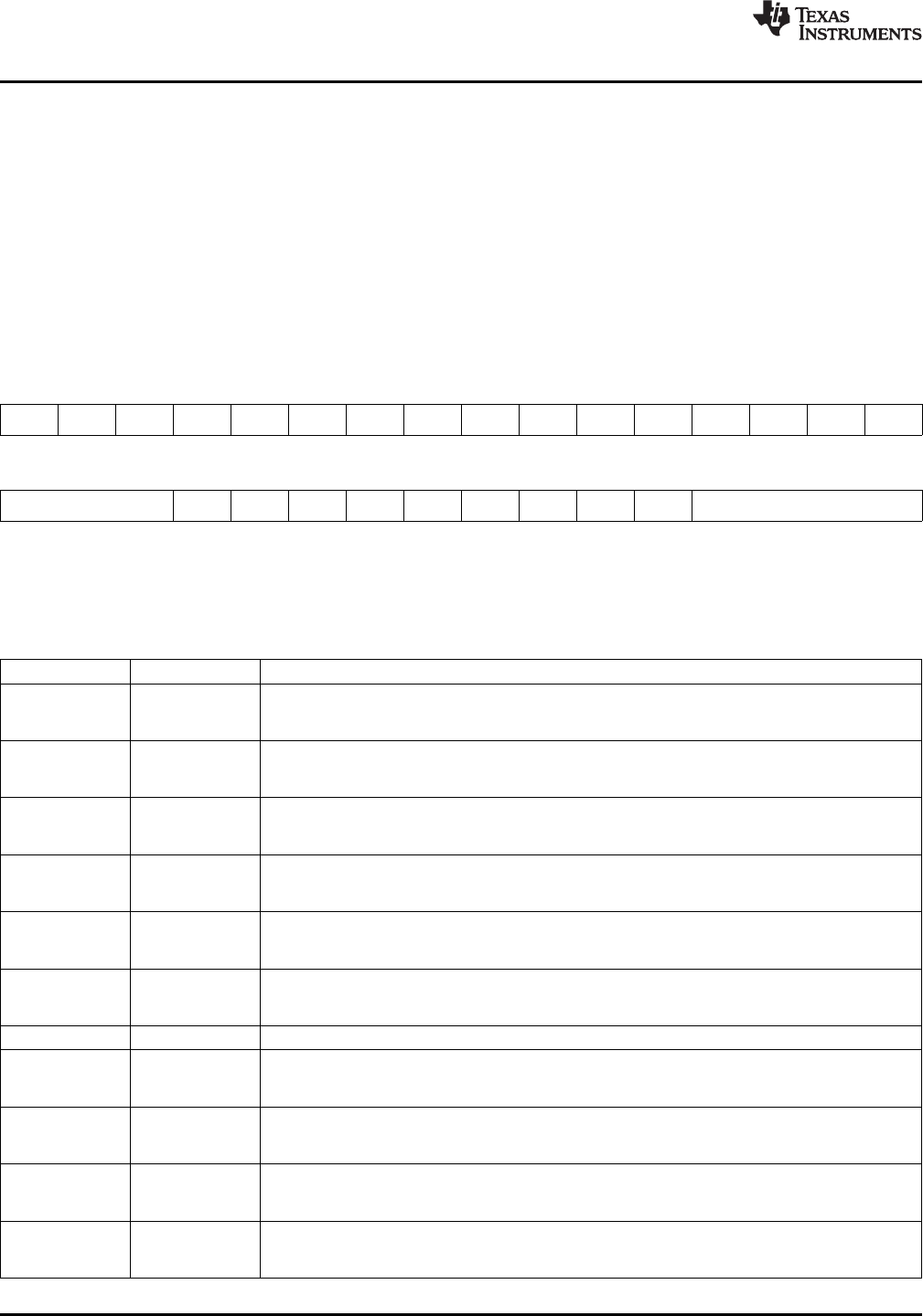
The SUSPSRC register format is shown in Figure 4-26. Brief details on the peripherals which correspond
to the register bits are listed in Table 4-45. When the associated SUSPSRC bit is ‘0’, the peripheral’s
emulation suspend signal is controlled by the ARM emulator and when set to ‘1’ it is controlled by the DSP
emulator.
31 30 29 28 27 26 25 24 23 22 21 20 19 18 17 16
CRGEN1 CRGEN0 TIMR2 TIMR1 TIMR0 GPIO PWM1 PWM0 SPI UART2 UART1 UART0 I2C MCASP1 MCASP0
RSV
SRC SRC SRC SRC SRC SRC SRC SRC SRC SRC SRC SRC SRC SRC SRC
R/W-0 R/W-0 R/W-0 R/W-0 R/W-0 R/W-0 R-0 R/W-0 R/W-0 R/W-0 R/W-0 R/W-0 R/W-0 R/W-0 R/W-0 R/W-0
15 13 12 11 10 9 8 7 6 5 4 3 0
HPI EMAC USB VDCE TSIF1 TSIF0 VPIF
RESERVED RSV RSV RESERVED
SRC SRC SRC SRC SRC SRC SRC
R-000 R/W-0 R-0 R/W-0 R/W-0 R/W-0 R/W-0 R/W-0 R-0 R/W-0 R-0000
LEGEND: R/W = Read/Write; R = Read only; -n = value after reset
Figure 4-26. SUSPSRC Register
Table 4-45. SUSPSRC Register Bit Descriptions
BIT NAME DESCRIPTION
Clock Recovery Generator 1 Emulation Suspend Source.
31 CRGEN1SRC 0 = ARM emulation suspend.
1 = DSP emulation suspend.
Clock Recovery Generator 0 Emulation Suspend Source.
30 CRGEN0SRC 0 = ARM emulation suspend.
1 = DSP emulation suspend.
Timer2 (WD Timer) Emulation Suspend Source.
29 TIMR2SRC 0 = ARM emulation suspend.
1 = DSP emulation suspend.
Timer1 Emulation Suspend Source.
28 TIMR1SRC 0 = ARM emulation suspend.
1 = DSP emulation suspend.
Timer0 Emulation Suspend Source.
27 TIMR0SRC 0 = ARM emulation suspend.
1 = DSP emulation suspend.
GPIO Emulation Suspend Source.
26 GPIOSRC 0 = ARM emulation suspend.
1 = DSP emulation suspend.
25 RSV Reserved. Read returns "0".
PWM1 Emulation Suspend Source.
24 PWM1SRC 0 = ARM emulation suspend.
1 = DSP emulation suspend.
PWM0 Emulation Suspend Source.
23 PWM0SRC 0 = ARM emulation suspend.
1 = DSP emulation suspend.
SPI Emulation Suspend Source.
22 SPISRC 0 = ARM emulation suspend.
1 = DSP emulation suspend.
UART2 Emulation Suspend Source.
21 UART2SRC 0 = ARM emulation suspend.
1 = DSP emulation suspend.
130 Device Configurations Copyright © 2009–2012, Texas Instruments Incorporated
Submit Documentation Feedback
Product Folder Link(s): TMS320DM6467T