
Datasheet


Table Of Contents
- 1 Digital Media System-on-Chip (DMSoC)
- Table of Contents
- 2 Revision History
- 3 Device Overview
- 3.1 Device Characteristics
- 3.2 Device Compatibility
- 3.3 ARM Subsystem
- 3.3.1 ARM926EJ-S RISC CPU
- 3.3.2 CP15
- 3.3.3 MMU
- 3.3.4 Caches and Write Buffer
- 3.3.5 Tightly Coupled Memory (TCM)
- 3.3.6 Advanced High-Performance Bus (AHB)
- 3.3.7 Embedded Trace Macrocell (ETM) and Embedded Trace Buffer (ETB)
- 3.3.8 ARM Memory Mapping
- 3.3.9 Peripherals
- 3.3.10 PLL Controller (PLLC)
- 3.3.11 Power and Sleep Controller (PSC)
- 3.3.12 ARM Interrupt Controller (AINTC)
- 3.3.13 System Module
- 3.3.14 Power Management
- 3.4 DSP Subsystem
- 3.5 Memory Map Summary
- 3.6 Pin Assignments
- 3.7 Terminal Functions
- 3.8 Device Support
- 3.9 Documentation Support
- 3.10 Community Resources
- 4 Device Configurations
- 4.1 System Module Registers
- 4.2 Power Considerations
- 4.3 Clock Considerations
- 4.4 Boot Sequence
- 4.5 Configurations At Reset
- 4.6 Configurations After Reset
- 4.7 Multiplexed Pin Configurations
- 4.7.1 Pin Muxing Selection At Reset
- 4.7.2 Pin Muxing Selection After Reset
- 4.7.3 Pin Multiplexing Details
- 4.7.3.1 PCI, HPI, EMIFA, and ATA Pin Muxing
- 4.7.3.2 PWM Signal Muxing
- 4.7.3.3 TSIF0 Input Signal Muxing (Serial/Parallel)
- 4.7.3.4 TSIF0 Output Signal Muxing (Serial/Parallel)
- 4.7.3.5 TSIF1 Input Signal Muxing (Serial Only)
- 4.7.3.6 TSIF1 Output Signal Muxing (Serial Only)
- 4.7.3.7 CRGEN Signal Muxing
- 4.7.3.8 UART0 Pin Muxing
- 4.7.3.9 UART1 Pin Muxing
- 4.7.3.10 UART2 Pin Muxing
- 4.7.3.11 ARM/DSP Communications Interrupts
- 4.7.3.12 Emulation Control
- 4.8 Debugging Considerations
- 5 System Interconnect
- 6 Device Operating Conditions
- 7 Peripheral Information and Electrical Specifications
- 7.1 Parameter Information
- 7.2 Recommended Clock and Control Signal Transition Behavior
- 7.3 Power Supplies
- 7.4 External Clock Input From DEV_MXI/DEV_CLKIN and AUX_MXI/AUX_CLKIN Pins
- 7.5 Clock PLLs
- 7.6 Enhanced Direct Memory Access (EDMA3) Controller
- 7.7 Reset
- 7.8 Interrupts
- 7.9 External Memory Interface (EMIF)
- 7.10 DDR2 Memory Controller
- 7.10.1 DDR2 Memory Controller Electrical Data/Timing
- 7.10.2 DDR2 Interface
- 7.10.2.1 DDR2 Interface Schematic
- 7.10.2.2 Compatible JEDEC DDR2 Devices
- 7.10.2.3 PCB Stackup
- 7.10.2.4 Placement
- 7.10.2.5 DDR2 Keep Out Region
- 7.10.2.6 Bulk Bypass Capacitors
- 7.10.2.7 High-Speed Bypass Capacitors
- 7.10.2.8 Net Classes
- 7.10.2.9 DDR2 Signal Termination
- 7.10.2.10 VREF Routing
- 7.10.2.11 DDR2 CK and ADDR_CTRL Routing
- 7.11 Video Port Interface (VPIF)
- 7.12 Transport Stream Interface (TSIF)
- 7.13 Clock Recovery Generator (CRGEN)
- 7.14 Video Data Conversion Engine (VDCE)
- 7.15 Peripheral Component Interconnect (PCI)
- 7.16 Ethernet MAC (EMAC)
- 7.17 Management Data Input/Output (MDIO)
- 7.18 Host-Port Interface (HPI) Peripheral
- 7.19 USB 2.0 [see Note]
- 7.20 ATA Controller
- 7.21 VLYNQ
- 7.22 Multichannel Audio Serial Port (McASP0/1) Peripherals
- 7.23 Serial Peripheral Interface (SPI)
- 7.24 Universal Asynchronouse Receiver/Transmitter (UART)
- 7.25 Inter-Integrated Circuit (I2C)
- 7.26 Pulse Width Modulator (PWM)
- 7.27 Timers
- 7.28 General-Purpose Input/Output (GPIO)
- 7.29 IEEE 1149.1 JTAG
- 8 Mechanical Packaging and Orderable Information
TMS320DM6467T
www.ti.com
SPRS605C –JULY 2009–REVISED JUNE 2012
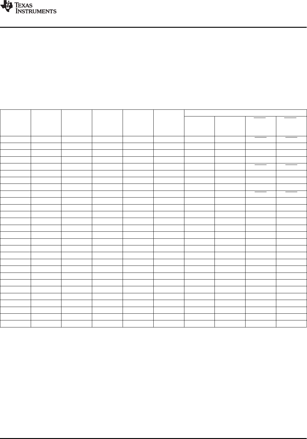
4.7.3.9 UART1 Pin Muxing
The UART1 module can operate as either a UART or IrDA/CIR interface. The UART1 pin muxing options
are shown in Table 4-35. When UART operation is selected, UART1CTL must be set to either ‘00’ for
UART with flow control or ‘01’ for UART without flow control signals. When IrDA/CIR operation is selected,
UART1CTL must be set to ‘10’ to use the IrDA/CIR signals. If UART1 is unused, then setting UART1CTL
= 11 muxes GPIO function onto all the pins. The UART1 pin functions may be overridden based on the
settings of TSPIMUX and TSPOMUX
Table 4-35. UART1 Pin Muxing
PIN FUNCTIONS
UTXD1/ URTS1 / UCTS1 /
URXD1/
TSPIMUX[1] TSPIMUX[0] TSPOMUX[1] TSPOMUX[0] UART1CTL[1] UART1CTL[0]
URCTX1/ UIRTX1/ USD1/
TS0_DIN7/
TS0_DOUT7/ TS0_WAITO/ TS0_EN_WAITO/
GP[23]
GP[24] GP[25] GP[26]
0 x 0 x 0 0 URXD1 UTXD1 URTS1 UCTS1
0 x 0 x 0 1 URXD1 UTXD1 GP[25] GP[26]
0 x 0 x 1 0 URXD1 URCTX1 UIRTX1 USD1
0 x 0 x 1 1 GP[23] GP[24] GP[25] GP[26]
0 x 1 0 0 0 URXD1 UTXD1 URTS1 UCTS1
0 x 1 0 0 1 URXD1 UTXD1 GP[25] GP[26]
0 x 1 0 1 0 URXD1 URCTX1 UIRTX1 USD1
0 x 1 0 1 1 GP[23] GP[24] GP[25] GP[26]
0 x 1 1 0 0 URXD1 TS0_DOUT7 URTS1 UCTS1
0 x 1 1 0 1 URXD1 TS0_DOUT7 GP[25] GP[26]
0 x 1 1 1 0 URXD1 TS0_DOUT7 UIRTX1 USD1
0 x 1 1 1 1 GP[23] TS0_DOUT7 GP[25] GP[26]
1 0 0 x 0 x URXD1 UTXD1 TS0_WAITO TS0_EN_WAITO
1 0 0 x 1 0 URXD1 URCTX1 TS0_WAITO TS0_EN_WAITO
1 0 0 x 1 1 GP[23] GP[24] TS0_WAITO TS0_EN_WAITO
1 0 1 0 0 x URXD1 UTXD1 TS0_WAITO TS0_EN_WAITO
1 0 1 0 1 0 URXD1 URCTX1 TS0_WAITO TS0_EN_WAITO
1 0 1 0 1 1 GP[23] GP[24] TS0_WAITO TS0_EN_WAITO
1 0 1 1 0 x URXD1 TS0_DOUT7 TS0_WAITO TS0_EN_WAITO
1 0 1 1 1 0 URXD1 TS0_DOUT7 TS0_WAITO TS0_EN_WAITO
1 0 1 1 1 1 GP[23] TS0_DOUT7 TS0_WAITO TS0_EN_WAITO
1 1 0 x 0 x TS0_DIN7 UTXD1 TS0_WAITO TS0_EN_WAITO
1 1 0 x 1 0 TS0_DIN7 URCTX1 TS0_WAITO TS0_EN_WAITO
1 1 0 x 1 1 TS0_DIN7 GP[24] TS0_WAITO TS0_EN_WAITO
1 1 1 0 0 x TS0_DIN7 UTXD1 TS0_WAITO TS0_EN_WAITO
1 1 1 0 1 0 TS0_DIN7 URCTX1 TS0_WAITO TS0_EN_WAITO
1 1 1 0 1 1 TS0_DIN7 GP[24] TS0_WAITO TS0_EN_WAITO
1 1 1 1 x x TS0_DIN7 TS0_DOUT7 TS0_WAITO TS0_EN_WAITO
Copyright © 2009–2012, Texas Instruments Incorporated Device Configurations 123
Submit Documentation Feedback
Product Folder Link(s): TMS320DM6467T