
Datasheet


Table Of Contents
- 1 Digital Media System-on-Chip (DMSoC)
- Table of Contents
- 2 Revision History
- 3 Device Overview
- 3.1 Device Characteristics
- 3.2 Device Compatibility
- 3.3 ARM Subsystem
- 3.3.1 ARM926EJ-S RISC CPU
- 3.3.2 CP15
- 3.3.3 MMU
- 3.3.4 Caches and Write Buffer
- 3.3.5 Tightly Coupled Memory (TCM)
- 3.3.6 Advanced High-Performance Bus (AHB)
- 3.3.7 Embedded Trace Macrocell (ETM) and Embedded Trace Buffer (ETB)
- 3.3.8 ARM Memory Mapping
- 3.3.9 Peripherals
- 3.3.10 PLL Controller (PLLC)
- 3.3.11 Power and Sleep Controller (PSC)
- 3.3.12 ARM Interrupt Controller (AINTC)
- 3.3.13 System Module
- 3.3.14 Power Management
- 3.4 DSP Subsystem
- 3.5 Memory Map Summary
- 3.6 Pin Assignments
- 3.7 Terminal Functions
- 3.8 Device Support
- 3.9 Documentation Support
- 3.10 Community Resources
- 4 Device Configurations
- 4.1 System Module Registers
- 4.2 Power Considerations
- 4.3 Clock Considerations
- 4.4 Boot Sequence
- 4.5 Configurations At Reset
- 4.6 Configurations After Reset
- 4.7 Multiplexed Pin Configurations
- 4.7.1 Pin Muxing Selection At Reset
- 4.7.2 Pin Muxing Selection After Reset
- 4.7.3 Pin Multiplexing Details
- 4.7.3.1 PCI, HPI, EMIFA, and ATA Pin Muxing
- 4.7.3.2 PWM Signal Muxing
- 4.7.3.3 TSIF0 Input Signal Muxing (Serial/Parallel)
- 4.7.3.4 TSIF0 Output Signal Muxing (Serial/Parallel)
- 4.7.3.5 TSIF1 Input Signal Muxing (Serial Only)
- 4.7.3.6 TSIF1 Output Signal Muxing (Serial Only)
- 4.7.3.7 CRGEN Signal Muxing
- 4.7.3.8 UART0 Pin Muxing
- 4.7.3.9 UART1 Pin Muxing
- 4.7.3.10 UART2 Pin Muxing
- 4.7.3.11 ARM/DSP Communications Interrupts
- 4.7.3.12 Emulation Control
- 4.8 Debugging Considerations
- 5 System Interconnect
- 6 Device Operating Conditions
- 7 Peripheral Information and Electrical Specifications
- 7.1 Parameter Information
- 7.2 Recommended Clock and Control Signal Transition Behavior
- 7.3 Power Supplies
- 7.4 External Clock Input From DEV_MXI/DEV_CLKIN and AUX_MXI/AUX_CLKIN Pins
- 7.5 Clock PLLs
- 7.6 Enhanced Direct Memory Access (EDMA3) Controller
- 7.7 Reset
- 7.8 Interrupts
- 7.9 External Memory Interface (EMIF)
- 7.10 DDR2 Memory Controller
- 7.10.1 DDR2 Memory Controller Electrical Data/Timing
- 7.10.2 DDR2 Interface
- 7.10.2.1 DDR2 Interface Schematic
- 7.10.2.2 Compatible JEDEC DDR2 Devices
- 7.10.2.3 PCB Stackup
- 7.10.2.4 Placement
- 7.10.2.5 DDR2 Keep Out Region
- 7.10.2.6 Bulk Bypass Capacitors
- 7.10.2.7 High-Speed Bypass Capacitors
- 7.10.2.8 Net Classes
- 7.10.2.9 DDR2 Signal Termination
- 7.10.2.10 VREF Routing
- 7.10.2.11 DDR2 CK and ADDR_CTRL Routing
- 7.11 Video Port Interface (VPIF)
- 7.12 Transport Stream Interface (TSIF)
- 7.13 Clock Recovery Generator (CRGEN)
- 7.14 Video Data Conversion Engine (VDCE)
- 7.15 Peripheral Component Interconnect (PCI)
- 7.16 Ethernet MAC (EMAC)
- 7.17 Management Data Input/Output (MDIO)
- 7.18 Host-Port Interface (HPI) Peripheral
- 7.19 USB 2.0 [see Note]
- 7.20 ATA Controller
- 7.21 VLYNQ
- 7.22 Multichannel Audio Serial Port (McASP0/1) Peripherals
- 7.23 Serial Peripheral Interface (SPI)
- 7.24 Universal Asynchronouse Receiver/Transmitter (UART)
- 7.25 Inter-Integrated Circuit (I2C)
- 7.26 Pulse Width Modulator (PWM)
- 7.27 Timers
- 7.28 General-Purpose Input/Output (GPIO)
- 7.29 IEEE 1149.1 JTAG
- 8 Mechanical Packaging and Orderable Information
TMS320DM6467T
www.ti.com
SPRS605C –JULY 2009–REVISED JUNE 2012
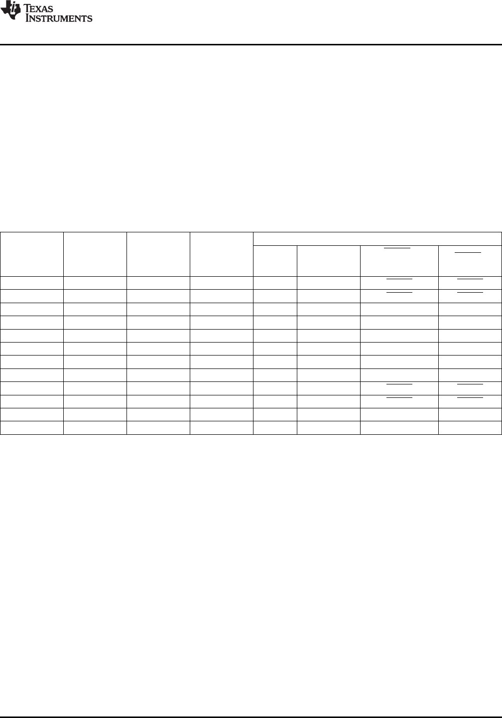
4.7.3.8 UART0 Pin Muxing
The UART0 module can operate as either a UART or IrDA/CIR interface. The UART0 pin muxing is
controlled by the UART0CTL bit field in the PINMUX1 register and the TSPOMUX, TSSIMUX, and
TSSOMUX bit fields in the PINMUX0 register. Muxing options are shown in Table 4-33 and Table 4-34.
When UART operation is selected, UART0CTL must be set to either ‘00’ for UART with modem signals or
‘01’ for UART without modem signals. When IrDA/CIR operation is selected, UART0CTL must be set to
‘1x’ to use the IrDA/CIR signals and the modem signal become GPIOs. A TSPOMUX setting of ‘1x’
overrides the modem control mux settings. UART0 can still be used as a UART without modem control or
in IrDA/CIR mode based on the UART0CTL bit field value. A TSSIMUX setting of ‘01’ overrides the UART
data and flow control settings and prevents UART0 from being used. The UART0 modem control pins may
be used as either TSIF 0 output or GPIO pins based on the TSPOMUX and UART0CTL settings. A
TSSOMUX setting of ‘11’ overrides the RIN function with the TS1_WAITIN function.
Table 4-33. UART0 Pin Muxing—Part 1
PIN FUNCTIONS
UTXD0/ URTS0 /
TSSIMUX[1] TSSIMUX[0] UART0CTL[1] UART0CTL[0]
URXD0/ UCTS0 /
URCTX0/ UIRTX0/
TS1_DIN USD0
TS1_PSTIN TS1_EN_WAITO
0 0 0 0 URXD0 UTXD0 URTS0 UCTS0
0 0 0 1 URXD0 UTXD0 URTS0 UCTS0
0 0 1 0 URXD0 URCTX0 UIRTX0 USD0
0 0 1 1 URXD0 URCTX0 UIRTX0 USD0
0 1 0 0 TS1_DIN TS1_PSTIN TS1_EN_WAITO –
0 1 0 1 TS1_DIN TS1_PSTIN TS1_EN_WAITO –
0 1 1 0 TS1_DIN TS1_PSTIN TS1_EN_WAITO –
0 1 1 1 TS1_DIN TS1_PSTIN TS1_EN_WAITO –
1 x 0 0 URXD0 UTXD0 URTS0 UCTS0
1 x 0 1 URXD0 UTXD0 URTS0 UCTS0
1 x 1 0 URXD0 URCTX0 UIRTX0 USD0
1 x 1 1 URXD0 URCTX0 UIRTX0 USD0
Copyright © 2009–2012, Texas Instruments Incorporated Device Configurations 121
Submit Documentation Feedback
Product Folder Link(s): TMS320DM6467T