
Datasheet


Table Of Contents
- 1 Digital Media System-on-Chip (DMSoC)
- Table of Contents
- 2 Revision History
- 3 Device Overview
- 3.1 Device Characteristics
- 3.2 Device Compatibility
- 3.3 ARM Subsystem
- 3.3.1 ARM926EJ-S RISC CPU
- 3.3.2 CP15
- 3.3.3 MMU
- 3.3.4 Caches and Write Buffer
- 3.3.5 Tightly Coupled Memory (TCM)
- 3.3.6 Advanced High-Performance Bus (AHB)
- 3.3.7 Embedded Trace Macrocell (ETM) and Embedded Trace Buffer (ETB)
- 3.3.8 ARM Memory Mapping
- 3.3.9 Peripherals
- 3.3.10 PLL Controller (PLLC)
- 3.3.11 Power and Sleep Controller (PSC)
- 3.3.12 ARM Interrupt Controller (AINTC)
- 3.3.13 System Module
- 3.3.14 Power Management
- 3.4 DSP Subsystem
- 3.5 Memory Map Summary
- 3.6 Pin Assignments
- 3.7 Terminal Functions
- 3.8 Device Support
- 3.9 Documentation Support
- 3.10 Community Resources
- 4 Device Configurations
- 4.1 System Module Registers
- 4.2 Power Considerations
- 4.3 Clock Considerations
- 4.4 Boot Sequence
- 4.5 Configurations At Reset
- 4.6 Configurations After Reset
- 4.7 Multiplexed Pin Configurations
- 4.7.1 Pin Muxing Selection At Reset
- 4.7.2 Pin Muxing Selection After Reset
- 4.7.3 Pin Multiplexing Details
- 4.7.3.1 PCI, HPI, EMIFA, and ATA Pin Muxing
- 4.7.3.2 PWM Signal Muxing
- 4.7.3.3 TSIF0 Input Signal Muxing (Serial/Parallel)
- 4.7.3.4 TSIF0 Output Signal Muxing (Serial/Parallel)
- 4.7.3.5 TSIF1 Input Signal Muxing (Serial Only)
- 4.7.3.6 TSIF1 Output Signal Muxing (Serial Only)
- 4.7.3.7 CRGEN Signal Muxing
- 4.7.3.8 UART0 Pin Muxing
- 4.7.3.9 UART1 Pin Muxing
- 4.7.3.10 UART2 Pin Muxing
- 4.7.3.11 ARM/DSP Communications Interrupts
- 4.7.3.12 Emulation Control
- 4.8 Debugging Considerations
- 5 System Interconnect
- 6 Device Operating Conditions
- 7 Peripheral Information and Electrical Specifications
- 7.1 Parameter Information
- 7.2 Recommended Clock and Control Signal Transition Behavior
- 7.3 Power Supplies
- 7.4 External Clock Input From DEV_MXI/DEV_CLKIN and AUX_MXI/AUX_CLKIN Pins
- 7.5 Clock PLLs
- 7.6 Enhanced Direct Memory Access (EDMA3) Controller
- 7.7 Reset
- 7.8 Interrupts
- 7.9 External Memory Interface (EMIF)
- 7.10 DDR2 Memory Controller
- 7.10.1 DDR2 Memory Controller Electrical Data/Timing
- 7.10.2 DDR2 Interface
- 7.10.2.1 DDR2 Interface Schematic
- 7.10.2.2 Compatible JEDEC DDR2 Devices
- 7.10.2.3 PCB Stackup
- 7.10.2.4 Placement
- 7.10.2.5 DDR2 Keep Out Region
- 7.10.2.6 Bulk Bypass Capacitors
- 7.10.2.7 High-Speed Bypass Capacitors
- 7.10.2.8 Net Classes
- 7.10.2.9 DDR2 Signal Termination
- 7.10.2.10 VREF Routing
- 7.10.2.11 DDR2 CK and ADDR_CTRL Routing
- 7.11 Video Port Interface (VPIF)
- 7.12 Transport Stream Interface (TSIF)
- 7.13 Clock Recovery Generator (CRGEN)
- 7.14 Video Data Conversion Engine (VDCE)
- 7.15 Peripheral Component Interconnect (PCI)
- 7.16 Ethernet MAC (EMAC)
- 7.17 Management Data Input/Output (MDIO)
- 7.18 Host-Port Interface (HPI) Peripheral
- 7.19 USB 2.0 [see Note]
- 7.20 ATA Controller
- 7.21 VLYNQ
- 7.22 Multichannel Audio Serial Port (McASP0/1) Peripherals
- 7.23 Serial Peripheral Interface (SPI)
- 7.24 Universal Asynchronouse Receiver/Transmitter (UART)
- 7.25 Inter-Integrated Circuit (I2C)
- 7.26 Pulse Width Modulator (PWM)
- 7.27 Timers
- 7.28 General-Purpose Input/Output (GPIO)
- 7.29 IEEE 1149.1 JTAG
- 8 Mechanical Packaging and Orderable Information
TMS320DM6467T
www.ti.com
SPRS605C –JULY 2009–REVISED JUNE 2012
4.7.3 Pin Multiplexing Details
This section discusses how to program each Pin Mux Register to select the desired peripheral functions
and pin muxing. See the individual pin mux sections for pin muxing details for a specific muxed pin.
For details on PINMUX0 and PINMUX1 registers, see Section 4.7.2, Pin Muxing Selection After Reset.
4.7.3.1 PCI, HPI, EMIFA, and ATA Pin Muxing
The PCI, HPI, EMIFA, and ATA signal muxing is determined by the value of the PCIEN, HPIEN, and
ATAEN bit fields in the PINMUX0 register. For more details on the actual pin functions, see Table 4-24
and Table 4-25.
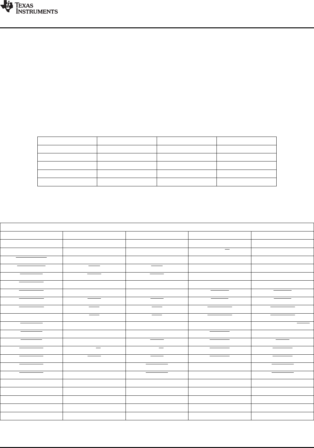
Table 4-24. PCIEN, HPIEN, and ATAEN Encoding
PCIEN HPIEN ATAEN PIN FUNCTIONS
0 0 0 EMIFA
0 0 1 EMIFA (NAND) and ATA
0 1 0 HPI (32-bit)
0 1 1 HPI (16-bit) and ATA
1 x x PCI
(1)
(1) In PCI mode (PCIEN = 1), the internal pullups/pulldowns (IPUs/IPDs) are disabled on all PCI pins and
it is recommended to have external pullup resistors on the PCI_RSV[5:0] pins. See Table 4-25 for the
actual PCI pin functions and any associated footnotes.
Table 4-25. PCI, HPI, EMIFA, and ATA Pin Muxing
PIN FUNCTIONS (WITH PCIEN, HPIEN, ATAEN VALUES)
1xx
(1)
010 011 000 001
PCI_CLK GP[10] GP[10] GP[10] GP[10]
PCI_IDSEL – HDDIR EM_R/W HDDIR
PCI_DEVSEL HCNTL1 HCNTL1 EM_BA[1] EM_BA[1]
PCI_FRAME HINT HINT EM_BA[0] EM_BA[0]
PCI_IRDY HRDY HRDY EM_A[17] EM_A[17]/(CLE)
PCI_TRDY HHWIL HHWIL EM_A[16] EM_A[16]/(ALE)
PCI_STOP HCNTL0 HCNTL0 EM_WE EM_WE
PCI_SERR HDS1 HDS1 EM_OE EM_OE
PCI_PERR HCS HCS EM_DQM1 EM_DQM1
PCI_PAR HAS HAS EM_DQM0 EM_DQM0
PCI_INTA – – EM_WAIT2 EM_WAIT2/(RDY2/BSY2)
PCI_REQ GP[11] DMARQ EM_CS5 DMARQ
PCI_GNT GP[12] DACK EM_CS4 DACK
PCI_CBE3 HR/W HR/W EM_CS3 EM_CS3
PCI_CBE2 HDS2 HDS2 EM_CS2 EM_CS2
PCI_CBE1 GP[32] ATA_CS1 EM_A[19] ATA_CS1
PCI_CBE0 GP[33] ATA_CS0 EM_A[18] ATA_CS0
PCI_AD31 HD31 DD15 EM_A[15] DD15
PCI_AD30 HD30 DD14 EM_A[14] DD14
PCI_AD29 HD29 DD13 EM_A[13] DD13
PCI_AD28 HD28 DD12 EM_A[12] DD12
PCI_AD27 HD27 DD11 EM_A[11] DD11
(1) In PCI mode (PCIEN = 1), the internal pullups/pulldowns (IPUs/IPDs) are disabled on all PCI pins and it is recommended to have
external pullup resistors on the PCI_RSV[5:0] pins. For more detailed information on external pullup/pulldown resistors, see
Section 4.8.1, Pullup/Pulldown Resistors.
Copyright © 2009–2012, Texas Instruments Incorporated Device Configurations 113
Submit Documentation Feedback
Product Folder Link(s): TMS320DM6467T