
Datasheet


Table Of Contents
- 1 Digital Media System-on-Chip (DMSoC)
- Table of Contents
- 2 Revision History
- 3 Device Overview
- 3.1 Device Characteristics
- 3.2 Device Compatibility
- 3.3 ARM Subsystem
- 3.3.1 ARM926EJ-S RISC CPU
- 3.3.2 CP15
- 3.3.3 MMU
- 3.3.4 Caches and Write Buffer
- 3.3.5 Tightly Coupled Memory (TCM)
- 3.3.6 Advanced High-Performance Bus (AHB)
- 3.3.7 Embedded Trace Macrocell (ETM) and Embedded Trace Buffer (ETB)
- 3.3.8 ARM Memory Mapping
- 3.3.9 Peripherals
- 3.3.10 PLL Controller (PLLC)
- 3.3.11 Power and Sleep Controller (PSC)
- 3.3.12 ARM Interrupt Controller (AINTC)
- 3.3.13 System Module
- 3.3.14 Power Management
- 3.4 DSP Subsystem
- 3.5 Memory Map Summary
- 3.6 Pin Assignments
- 3.7 Terminal Functions
- 3.8 Device Support
- 3.9 Documentation Support
- 3.10 Community Resources
- 4 Device Configurations
- 4.1 System Module Registers
- 4.2 Power Considerations
- 4.3 Clock Considerations
- 4.4 Boot Sequence
- 4.5 Configurations At Reset
- 4.6 Configurations After Reset
- 4.7 Multiplexed Pin Configurations
- 4.7.1 Pin Muxing Selection At Reset
- 4.7.2 Pin Muxing Selection After Reset
- 4.7.3 Pin Multiplexing Details
- 4.7.3.1 PCI, HPI, EMIFA, and ATA Pin Muxing
- 4.7.3.2 PWM Signal Muxing
- 4.7.3.3 TSIF0 Input Signal Muxing (Serial/Parallel)
- 4.7.3.4 TSIF0 Output Signal Muxing (Serial/Parallel)
- 4.7.3.5 TSIF1 Input Signal Muxing (Serial Only)
- 4.7.3.6 TSIF1 Output Signal Muxing (Serial Only)
- 4.7.3.7 CRGEN Signal Muxing
- 4.7.3.8 UART0 Pin Muxing
- 4.7.3.9 UART1 Pin Muxing
- 4.7.3.10 UART2 Pin Muxing
- 4.7.3.11 ARM/DSP Communications Interrupts
- 4.7.3.12 Emulation Control
- 4.8 Debugging Considerations
- 5 System Interconnect
- 6 Device Operating Conditions
- 7 Peripheral Information and Electrical Specifications
- 7.1 Parameter Information
- 7.2 Recommended Clock and Control Signal Transition Behavior
- 7.3 Power Supplies
- 7.4 External Clock Input From DEV_MXI/DEV_CLKIN and AUX_MXI/AUX_CLKIN Pins
- 7.5 Clock PLLs
- 7.6 Enhanced Direct Memory Access (EDMA3) Controller
- 7.7 Reset
- 7.8 Interrupts
- 7.9 External Memory Interface (EMIF)
- 7.10 DDR2 Memory Controller
- 7.10.1 DDR2 Memory Controller Electrical Data/Timing
- 7.10.2 DDR2 Interface
- 7.10.2.1 DDR2 Interface Schematic
- 7.10.2.2 Compatible JEDEC DDR2 Devices
- 7.10.2.3 PCB Stackup
- 7.10.2.4 Placement
- 7.10.2.5 DDR2 Keep Out Region
- 7.10.2.6 Bulk Bypass Capacitors
- 7.10.2.7 High-Speed Bypass Capacitors
- 7.10.2.8 Net Classes
- 7.10.2.9 DDR2 Signal Termination
- 7.10.2.10 VREF Routing
- 7.10.2.11 DDR2 CK and ADDR_CTRL Routing
- 7.11 Video Port Interface (VPIF)
- 7.12 Transport Stream Interface (TSIF)
- 7.13 Clock Recovery Generator (CRGEN)
- 7.14 Video Data Conversion Engine (VDCE)
- 7.15 Peripheral Component Interconnect (PCI)
- 7.16 Ethernet MAC (EMAC)
- 7.17 Management Data Input/Output (MDIO)
- 7.18 Host-Port Interface (HPI) Peripheral
- 7.19 USB 2.0 [see Note]
- 7.20 ATA Controller
- 7.21 VLYNQ
- 7.22 Multichannel Audio Serial Port (McASP0/1) Peripherals
- 7.23 Serial Peripheral Interface (SPI)
- 7.24 Universal Asynchronouse Receiver/Transmitter (UART)
- 7.25 Inter-Integrated Circuit (I2C)
- 7.26 Pulse Width Modulator (PWM)
- 7.27 Timers
- 7.28 General-Purpose Input/Output (GPIO)
- 7.29 IEEE 1149.1 JTAG
- 8 Mechanical Packaging and Orderable Information
TMS320DM6467T
SPRS605C –JULY 2009–REVISED JUNE 2012
www.ti.com
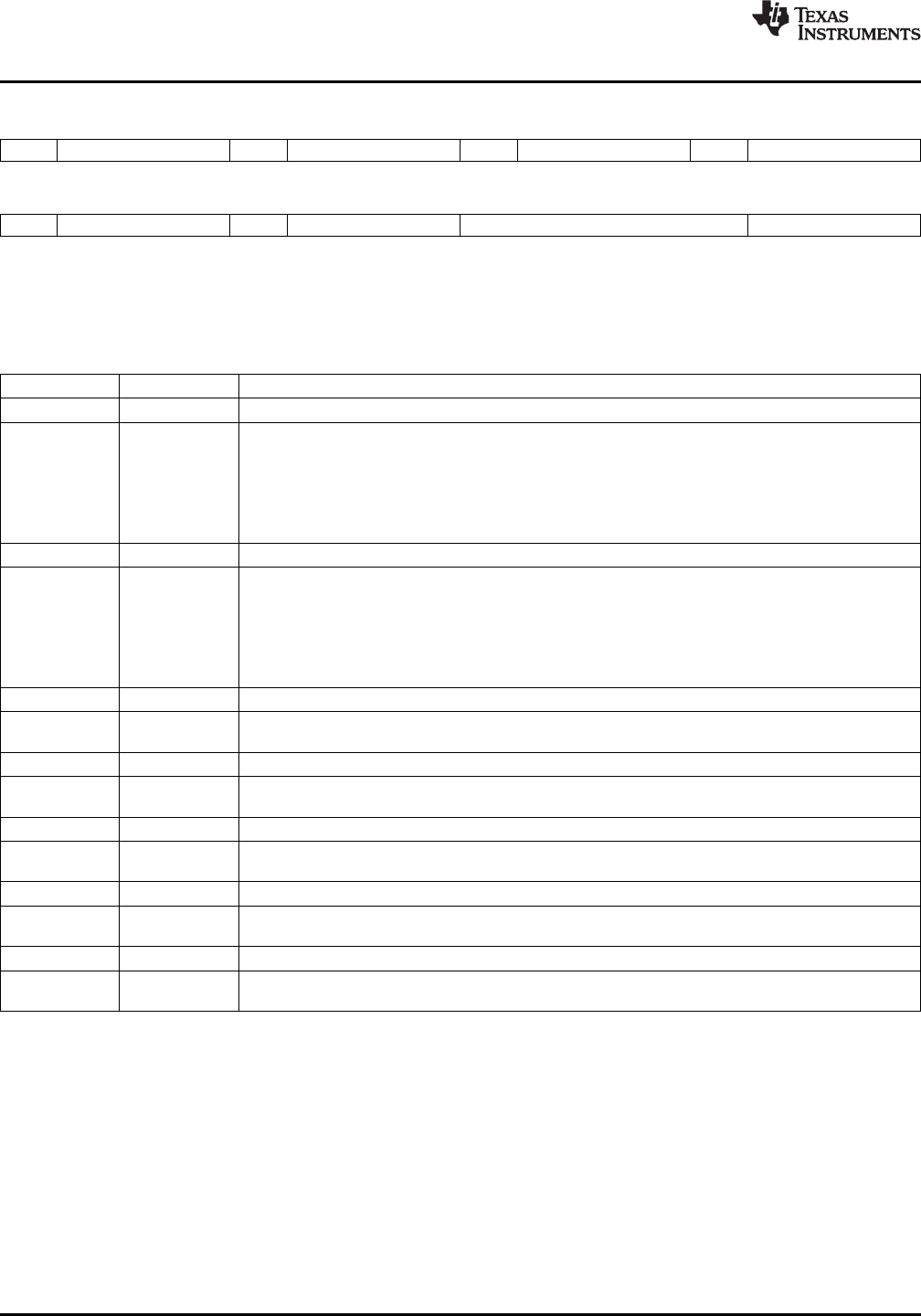
31 30 28 27 26 24 23 22 20 19 18 16
RSV VDCEP RSV PCIP RSV HPIP RSV VLYNQP
R-0 R/W-100 R-0 R/W-110 R-0 R/W-110 R-0 R/W-101
15 14 12 11 10 8 7 3 2 0
RSV ATAP RSV USBP RESERVED EMACP
R-0 R/W-101 R-0 R/W-101 R-0000 0 R/W-101
LEGEND: R/W = Read/Write; R = Read only; -n = value after reset
Figure 4-12. MSTPRI1 Register [0x01C4 0040]
Table 4-16. MSTPRI1 Register Bit Descriptions
BIT NAME DESCRIPTION
31 RSV Reserved. Read returns "0".
30:28 VDCEP VDCE master port priority in System Infrastructure.
000 = Priority 0 (Highest) 100 = Priority 4 [Default]
001 = Priority 1 101 = Priority 5
010 = Priority 2 110 = Priority 6
011 = Priority 3 111 = Priority 7 (Lowest)
27 RSV Reserved. Read returns "0".
26:24 PCIP PCI master port priority in System Infrastructure.
000 = Priority 0 (Highest) 100 = Priority 4
001 = Priority 1 101 = Priority 5
010 = Priority 2 110 = Priority 6 [Default]
011 = Priority 3 111 = Priority 7 (Lowest)
23 RSV Reserved. Read returns "0".
HPI master port priority in System Infrastructure. Same priority 0–7 selection as above.
22:20 HPIP
"110" = Priority 6 [default].
19 RSV Reserved. Read returns "0".
VLYNQ master port priority in System Infrastructure. Same priority 0–7 selection as above.
18:16 VLYNQP
"110" = Priority 6 [default].
15 RSV Reserved. Read returns "0".
ATA master port priority in System Infrastructure. Same priority 0–7 selection as above.
14:12 ATAP
"101" = Priority 5 [default].
11 RSV Reserved. Read returns "0".
USB master port priority in System Infrastructure. Same priority 0–7 selection as above.
10:8 USBP
"101" = Priority 5 [default].
7:3 RESERVED Reserved. Read returns "0".
EMAC master port priority in System Infrastructure. Same priority 0–7 selection as above.
2:0 EMACP
"101" = Priority 5 [default].
104 Device Configurations Copyright © 2009–2012, Texas Instruments Incorporated
Submit Documentation Feedback
Product Folder Link(s): TMS320DM6467T