
Datasheet


Table Of Contents
- FEATURES
- DESCRIPTION
- DESCRIPTION (Continued)
- FUNCTIONAL BLOCK DIAGRAM
- ABSOLUTE MAXIMUM RATINGS
- DISSIPATION RATINGS
- RECOMMENDED OPERATING CONDITIONS
- REFERENCE CLOCK (REFCLK) TIMING REQUIREMENTS
- TTL ELECTRICAL CHARACTERISTICS
- TRANSMITTER/RECEIVER CHARACTERISTICS
- LVTTL OUTPUT SWITCHING CHARACTERISTICS
- TRANSMITTER TIMING REQUIREMENTS
- APPLICATION INFORMATION
- Revision History
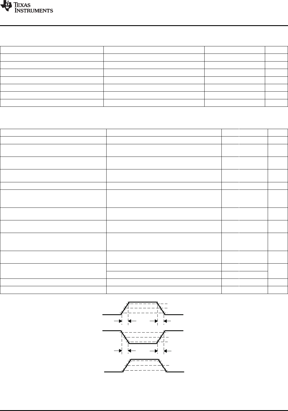
80%
50%
20%
t
r
t
r
t
f
t
f
80%
50%
20%
~
V
~
V
~
V
~
V
80%
20%
0V
~
1V
~
–1V
TX+
TX–
VOD
TLK1221
www.ti.com
....................................................................................................................................... SLLS713C –FEBRUARY 2007–REVISED SEPTEMBER 2009
TTL ELECTRICAL CHARACTERISTICS
over recommended operating conditions (unless otherwise noted)
PARAMETER TEST CONDITIONS MIN TYP MAX UNIT
V
OH
High-level output voltage I
OH
= –400 μA V
DD
– 0.2 2.3 V
V
OL
Low-level output voltage I
OL
= 1 mA GND 0.25 0.5 V
V
IH
High-level input voltage 1.7 3.6 V
V
IL
Low-level input voltage 0.8 V
I
IH
High-level input current V
DD
= 2.3 V, V
IN
= 2 V 40 μA
I
IL
Low-level input current V
DD
= 2.3 V, V
IN
= 0.4 V –40 μA
C
IN
Input capacitance 4 pF
TRANSMITTER/RECEIVER CHARACTERISTICS
over recommended operating conditions (unless otherwise noted)
PARAMETER TEST CONDITIONS MIN TYP MAX UNIT
VOD = |TxD – TxN| Rt = 50 Ω 600 850 1100 mV
Transmit common mode voltage
V
(CM)
Rt = 50 Ω 1000 1250 1400 mV
range
Receiver input voltage requirement,
200 1600 mV
VID = |RxP – RxN|
Receiver common mode voltage
1000 1250 2250 mV
range, (RxP + RxN)/2
C
I
Receiver input capacitance 2 pF
Differential output jitter, random + deterministic, PRBS
t
(TJ)
Serial data total jitter (peak-to-peak) pattern, 0.24 UI
R
ω
= 125 MHz
Serial data deterministic jitter Differential output jitter, PRBS pattern, R
ω
= 125 MHz
t
(DJ)
0.12 UI
(peak-to-peak)
Differential signal rise, fall time (20% R
L
= 50 Ω, C
L
= 5 pF, see Figure 6 and Figure 8
t
r
, t
f
100 250 ps
to 80%)
Serial data jitter tolerance minimum
Differential input jitter, random + deterministic, R
ω
=
required eye opening, (per 0.25 UI
125 MHz
IEEE-802.3 specification)
Receiver data acquisition lock time
500 μs
from power up
0.75 UI jitter closure with random data ata 1.25 Gbps 256
Data relock time from application of
ns
valid input data stream
0.20 UI jitter closure with 01010.. data at 1.25 Gbps 128
t
d(Tx latency)
Tx latency See Figure 1 20 22 UI
t
d(Rx latency)
Rx latency See Figure 5 and Figure 7 18 24 UI
Figure 6. Differential and Common-Mode Output Voltage Definitions
Copyright © 2007–2009, Texas Instruments Incorporated Submit Documentation Feedback 9
Product Folder Link(s): TLK1221