
Datasheet


Table Of Contents
- FEATURES
- DESCRIPTION
- DESCRIPTION (Continued)
- FUNCTIONAL BLOCK DIAGRAM
- ABSOLUTE MAXIMUM RATINGS
- DISSIPATION RATINGS
- RECOMMENDED OPERATING CONDITIONS
- REFERENCE CLOCK (REFCLK) TIMING REQUIREMENTS
- TTL ELECTRICAL CHARACTERISTICS
- TRANSMITTER/RECEIVER CHARACTERISTICS
- LVTTL OUTPUT SWITCHING CHARACTERISTICS
- TRANSMITTER TIMING REQUIREMENTS
- APPLICATION INFORMATION
- Revision History
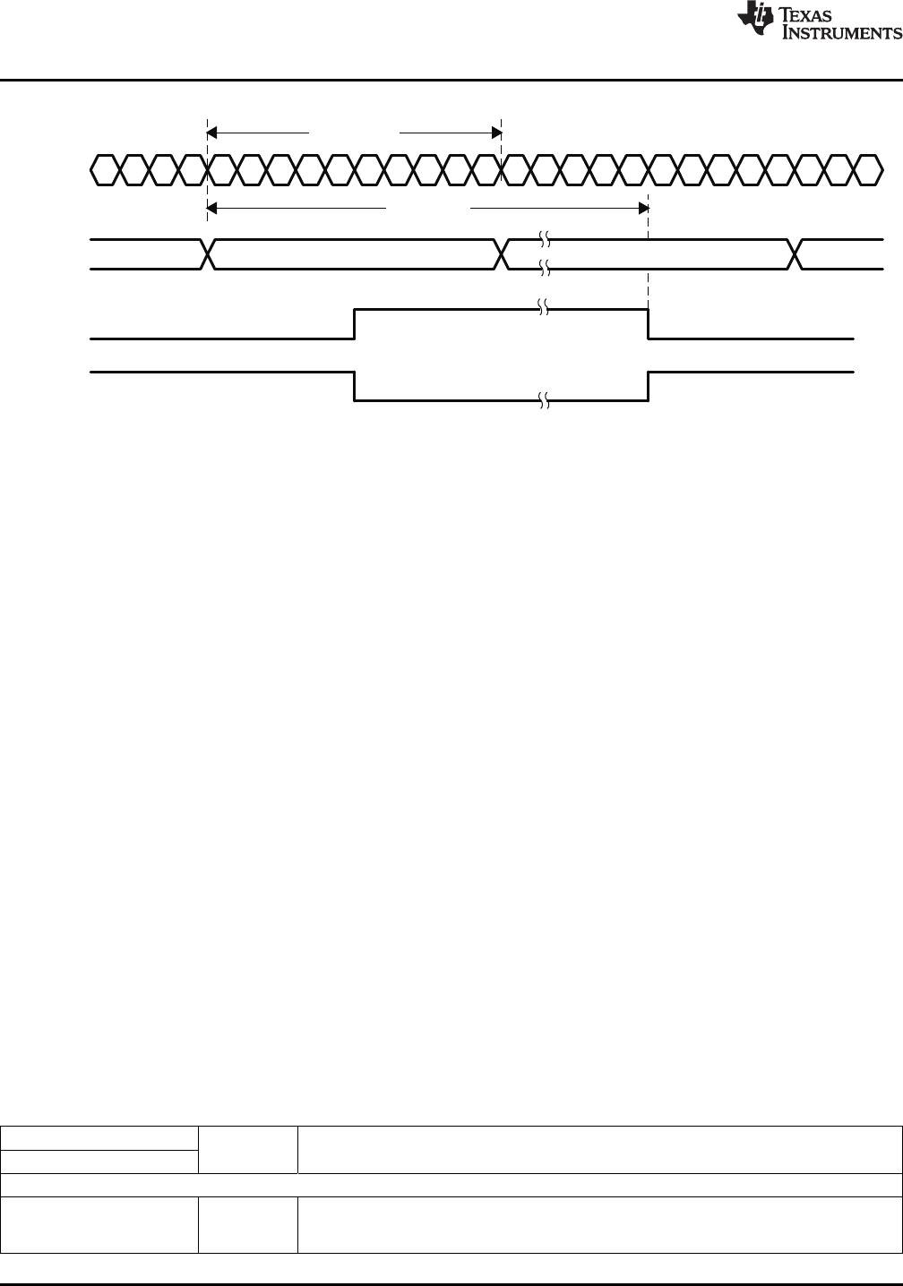
10-BitCode
RXP,RXN
RD(0–9)
RBC0
10-BitCode
t
d(Rx latency)
RBC1
TLK1221
SLLS713C –FEBRUARY 2007–REVISED SEPTEMBER 2009.......................................................................................................................................
www.ti.com
Figure 5. Receiver Latency, TBI Half-Rate Mode Shown
Testability
The loopback function provides for at-speed testing of the transmit/receive section of the circuitry. The enable
function allows for all circuitry to be disabled so that an Iddq test can be performed. The PRBS function also
allows for built-in self-test (BIST).
Loopback Testing
The transceiver can provide a self-test function by enabling (LOOPEN to high level) the internal loopback path.
Enabling this function causes serial transmitted data to be routed internally to the receiver. The parallel data
output can be compared to the parallel input data for functional verification. (The external differential output is
held in a high-impedance state during the loopback testing.)
ENABLE Function
When held low, ENABLE disables all quiescent power in both analog and digital circuitry. This allows an
ultralow-power idle state when the link is not active.
PRBS Function
These devices have a built-in 2
7
– 1 PRBS function. When the PRBSEN control bit is set high, the PRBS test is
enabled. A PRBS is generated and fed into the 10-bit parallel transmitter input bus. Data from the normal parallel
input source is ignored during PRBS test mode. The PRBS pattern is then fed through the transmit circuitry as if
it were normal data and sent out to the transmitter. The output can be sent to a bit error rate tester (BERT) or to
the receiver of another TLK1221. Because the PRBS is not really random and is really a predetermined
sequence of ones and zeros, the data can be captured and checked for errors by a BERT. These devices also
have a built-in BERT function on the receiver side that is enabled by PRBSEN. It can receive a PRBS pattern
and check for errors, and then report the errors by forcing the SYNC/PASS terminal low. The PRBS testing
supports two modes (normal and latched), which are controlled by the SYNCEN input. When SYNCEN is low,
the result of the PRBS bit-error-rate test is passed to the SYNC/PASS terminal. When SYNCEN is high, the
result of the PRBS verification is latched on the SYNC/PASS output (i.e., a single failure forces SYNC/PASS to
remain low).
Table 2. PIN FUNCTIONS
PIN
I/O DESCRIPTION
NAME NO.
SIGNAL
Differential output transmit. TXP and TXN are differential serial outputs that interface to a
TXP 38 PECL
copper or an optical I/F module. TXP and TXN are put in a high-impedance state when
TXN 39 O
LOOPEN is high and are active when LOOPEN is low.
6 Submit Documentation Feedback Copyright © 2007–2009, Texas Instruments Incorporated
Product Folder Link(s): TLK1221