
Datasheet


Table Of Contents
- FEATURES
- DESCRIPTION
- DESCRIPTION (Continued)
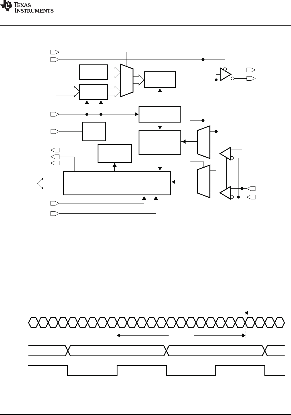
- FUNCTIONAL BLOCK DIAGRAM
- ABSOLUTE MAXIMUM RATINGS
- DISSIPATION RATINGS
- RECOMMENDED OPERATING CONDITIONS
- REFERENCE CLOCK (REFCLK) TIMING REQUIREMENTS
- TTL ELECTRICAL CHARACTERISTICS
- TRANSMITTER/RECEIVER CHARACTERISTICS
- LVTTL OUTPUT SWITCHING CHARACTERISTICS
- TRANSMITTER TIMING REQUIREMENTS
- APPLICATION INFORMATION
- Revision History
2:1
MUX
PRBS
Generator
10Bit
Registers
TD(0–9)
PRBSEN
LOOPEN
Parallelto
Serial
PhaseGenerator
Clock
REFCLK
Control
Logic
ENABLE
Interpolator
and
ClockExtraction
PRBS
Verification
SerialtoParallel
and
CommaDetect
Clock
RBC1
RBC0
SYNC/PASS
RD(0–9)
SYNCEN
2:1
MUX
2:1
MUX
Clock
Data
TXP
TXN
RXP
RXN
RBCMODE
10-BitCode
TXP,TXN
REFCLK
t
d(Tx latency)
10-BitCode
b9
TD(0–9)
TLK1221
www.ti.com
....................................................................................................................................... SLLS713C –FEBRUARY 2007–REVISED SEPTEMBER 2009
FUNCTIONAL BLOCK DIAGRAM
Detailed Description
In the TBI mode, the transmitter portion registers incoming 10-bit-wide data words (8b/10b encoded data,
TD0–TD9) on the rising edge of REFCLK. REFCLK is also used by the serializer, which multiplies the clock by a
factor of 10, providing a signal that is fed to the shift register. The 8b/10b encoded data is transmitted
sequentially, bits 0 through 9, over the differential high-speed I/O channel.
Transmission Latency
Data transmission latency is defined as the delay from the initial 10-bit word load to the serial transmission of
bit 9. The minimum latency in TBI mode is 20 bit times. The maximum latency in TBI mode is 22 bit times.
Figure 1. Transmitter Latency, Full-Rate Mode
Copyright © 2007–2009, Texas Instruments Incorporated Submit Documentation Feedback 3
Product Folder Link(s): TLK1221