
Datasheet


THS6226
SBOS499C –JANUARY 2011–REVISED APRIL 2011
www.ti.com
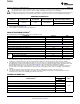
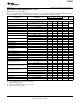
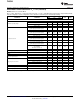
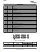
ELECTRICAL CHARACTERISTICS: V
S
= +12V (continued)
Boldface limits are tested at +25°C.
At T
A
= +25°C, with R
MATCH
= 10.2Ω, transformer turn ratio 1:1.4, R
L
= 100Ω differential at transformer output, Full Bias Mode,
and active impedance circuit configuration, unless otherwise noted. Each port is tested independently.
THS6226IRHB
TEST
PARAMETER CONDITIONS MIN TYP MAX UNIT LEVEL
(1)
POWER SUPPLY
Class AB +10 +12 +15 V A
–40°C to +85°C +10 +15 V B
Maximum operating voltage
Class H +10 +12 +12.5 V B
–40°C to +85°C +10 +12.5 B
Per port, full bias, class H enable
22.5 23.5 24.5 mA A
(power supply connected together)
–40°C to +85°C 21.8 25.2 mA B
Per port, full bias, class H disable
22.0 23.0 24.0 mA A
(power supply connected together)
–40°C to +85°C 21.3 24.7 mA B
Bias current step 1.0 mA C
Per port, low bias, class H disable
7.2 7.6 8 mA A
I
S+
quiescent current
(power supply connected together)
–40°C to +85°C 6.9 8.3 mA B
Per port, line termination mode
(B9 = B8 =B7 = B6 = 0) 4.4 mA C
(power supply connected together)
Both ports, main amplifiers and
class H disable 1.7 2.2 mA A
(B9 = B8 = B7 = B6 = 0)
–40°C to +85°C 2.3 mA B
Power-supply rejection (PSRR) Differential, from +12V, GND 60 70 dB A
–40°C to +85°C 58 dB B
LOGIC
Logic 1, with respect to GND
(5)
1.9 V C
Logic pin logic threshold
Logic 0, with respect to GND
(5)
0.8 V C
Logic X = 0.5V (logic 0) 10 25 μA A
–40°C to +85°C 30 μA B
Logic pin quiescent current
Logic X = 3.3V (logic 1) 66 125 μA A
–40°C to +85°C 130 μA B
Turn-on time delay (t
ON
) Time for I
S
to reach 50% of final value 1 μs C
Turn-off time delay (t
OFF
) Time for I
S
to reach 50% of final value 1 μs C
Logic pin input impedance 50 || 1 kΩ || pF C
(5) The GND pin usable range is from V
S–
to (V
S+
– 5V).
4 Submit Documentation Feedback Copyright © 2011, Texas Instruments Incorporated
Product Folder Link(s): THS6226