
Datasheet


THS6226
SBOS499C –JANUARY 2011–REVISED APRIL 2011
www.ti.com
This integrated circuit can be damaged by ESD. Texas Instruments recommends that all integrated circuits be handled with
appropriate precautions. Failure to observe proper handling and installation procedures can cause damage.
ESD damage can range from subtle performance degradation to complete device failure. Precision integrated circuits may be more
susceptible to damage because very small parametric changes could cause the device not to meet its published specifications.
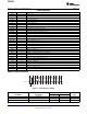
ORDERING INFORMATION
(1)
PACKAGE
PRODUCT
(2)
PACKAGE-LEAD DESIGNATOR PACKAGE MARKING TRANSPORT MEDIA, QUANTITY
THS6226IRHBT Tape and Reel, 250
VQFN-32 RHB THS6226IRHB
THS6226IRHBR Tape and Reel, 3000
(1) For the most current package and ordering information, see the Package Option Addendum at the end of this document, or visit the
device product folder at www.ti.com.
(2) The PowerPAD is electrically isolated from all other pins.
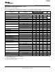
ABSOLUTE MAXIMUM RATINGS
(1)
Over operating free-air temperature range, unless otherwise noted.
PARAMETER THS6226 UNIT
Supply voltage, GND to V
S+
, class AB only 15 V
Supply voltage, GND to V
S+
, class H only 12.5 V
Input voltage, V
I
15 V
Output current, I
O
: static dc
(2)
±100 mA
Continuous power dissipation See Thermal Information table
Normal storage temperature –40 to +85 °C
Maximum junction temperature, any condition, T
J
(3)
+150 °C
Maximum junction temperature, continuous operation, long-term reliability, T
J
(4)
+130 °C
Storage temperature range, T
STG
–65 to +150 °C
Human body model (HBM) 2000 V
ESD
Charged device model (CDM) 500 V
ratings:
Machine model (MM) 100 V
(1) Stresses above those listed under absolute maximum ratings may cause permanent damage to the device. These are stress ratings
only, and functional operation of the device at these or any other conditions beyond those indicated under recommended operating
conditions is not implied. Exposure to absolute maximum rated conditions for extended periods may degrade device reliability.
(2) The THS6226 incorporates a PowerPAD on the underside of the chip. This acts as a heatsink and must be connected to a thermally
dissipating plane for proper power dissipation. Failure to do so may result in exceeding the maximum junction temperature which could
permanently damage the device. See TI Technical Brief SLMA002 for more information about utilizing the PowerPAD
thermally-enhanced package. Under high-frequency ac operation (> 10kHz), the short-term output current capability is much greater
than the continuous dc output current rating. This short-term output current rating is about 8.5x the dc capability, or approximately
±850mA.
(3) The absolute maximum junction temperature under any condition is limited by the constraints of the silicon process.
(4) The absolute maximum junction temperature for continuous operation is limited by the package constraints. Operation above this
temperature may result in reduced reliability and/or lifetime of the device.
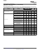
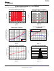
THERMAL INFORMATION
THS6226
THERMAL METRIC
(1)
RHB UNITS
32 PINS
θ
JA
Junction-to-ambient thermal resistance 35.1
θ
JCtop
Junction-to-case (top) thermal resistance 22.1
θ
JB
Junction-to-board thermal resistance 7.0
°C/W
ψ
JT
Junction-to-top characterization parameter 0.3
ψ
JB
Junction-to-board characterization parameter 6.9
θ
JCbot
Junction-to-case (bottom) thermal resistance 1.3
(1) For more information about traditional and new thermal metrics, see the IC Package Thermal Metrics application report, SPRA953.
2 Submit Documentation Feedback Copyright © 2011, Texas Instruments Incorporated
Product Folder Link(s): THS6226