
Datasheet


Table Of Contents
- FEATURES
- TYPICAL LEVEL-SHIFTER APPLICATIONS
- DESCRIPTION
- ABSOLUTE MAXIMUM RATINGS
- RECOMMENDED OPERATING CONDITIONS
- ELECTRICAL CHARACTERISTICS
- TIMING REQUIREMENTS
- TIMING REQUIREMENTS
- TIMING REQUIREMENTS
- SWITCHING CHARACTERISTICS
- SWITCHING CHARACTERISTICS
- SWITCHING CHARACTERISTICS
- PRINCIPLES OF OPERATION
- PARAMETER MEASUREMENT INFORMATION
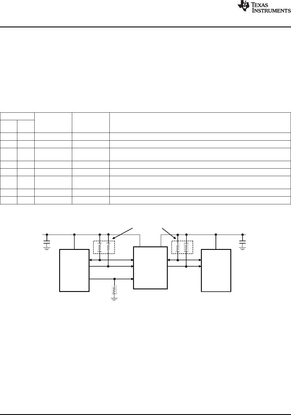
Master
I2C
Bus
I2C
Bus
Devices
1.8V
0.1!F
3.3V
V
CCA
V
CCB
SDA_A SDA_B
SCL_A SCL_B
OE
Optional Resistors
Design Notes:
OE can be tied directly to 1.8V (V ) to always be in ENABLE mode.
CCA
Master
I2C
Bus
I2C
Bus
Devices
1.8V
0.1!F
3.3V
V
CCA
V
CCB
SDA_A SDA_B
SCL_A SCL_B
OE
Optional Resistors
Design Notes:
TCA9406
SCPS221B –OCTOBER 2010–REVISED JUNE 2013
www.ti.com
The TCA9406 is not a bus buffer like the PCA9515B and PCA9517. The OE feature can be utilized to isolate
one side of the bus from the other by placing both sides into a high impedence state.
The Enable (OE) should be tied to GND through a pulldown resistor to ensure the high-impedance state
during power up or power down. The minimum value of the resistor is determined by the current-sourcing
capability of the driver.
ORDERING INFORMATION
For package and ordering information, see the Package Option Addendum at the end of this document.
PIN DESCRIPTION
NO.
NAME TYPE FUNCTION
DQM,
YZP
DCU
1 A1 SDA_B I/O Input/output B. Referenced to V
CCB
. Allow I2C_SDA configured to 2.5V/3.3V/5V
2 B1 GND GND Ground
A-port supply voltage. 1.65 V ≤ V
CCA
≤ 3.6 V and V
CCA
≤ V
CCB
. Configuration for
3 C1 V
CCA
PWR
SDA_A, SCL_A, and OE
4 D1 SDA_A I/O Input/output A. Referenced to V
CCA
. Allows I2C_SDA configured to 1.8V, 2.5V, 3.3V
5 D2 SCL_A I/O Input/output A. Referenced to V
CCA
. Allows I2C_SCL configured to 1.8V, 2.5V, 3.3V
Output enable (active High). Referenced to V
CCA
. Pull OE to LOW to place all outputs
6 C2 OE Input
in tri-state mode.
7 B2 V
CCB
PWR B-port supply voltage. 2.3 V ≤ V
CCB
≤ 5.5 V for SDA_B, SCL_B
8 A2 SCL_B I/O Input/output B. Referenced to V
CCB
. Allow I2C_SCL configured to 2.5V/3.3V/5V
TYPICAL OPERATING CIRCUIT
2 Submit Documentation Feedback Copyright © 2010–2013, Texas Instruments Incorporated
Product Folder Links: TCA9406