
Datasheet


Table Of Contents
- FEATURES
- DESCRIPTION/ORDERING INFORMATION
- DESCRIPTION/ORDERING INFORMATION (CONTINUED)
- ABSOLUTE MAXIMUM RATINGS
- RECOMMENDED OPERATING CONDITIONS
- ELECTRICAL CHARACTERISTICS
- I2C INTERFACE TIMING REQUIREMENTS
- RESET TIMING REQUIREMENTS
- SWITCHING CHARACTERISTICS
- TYPICAL CHARACTERISTICS
- PARAMETER MEASUREMENT INFORMATION
- APPLICATION INFORMATION
- REVISION HISTORY
TCA6424A
www.ti.com
SCPS193B –JULY 2010–REVISED SEPTEMBER 2010
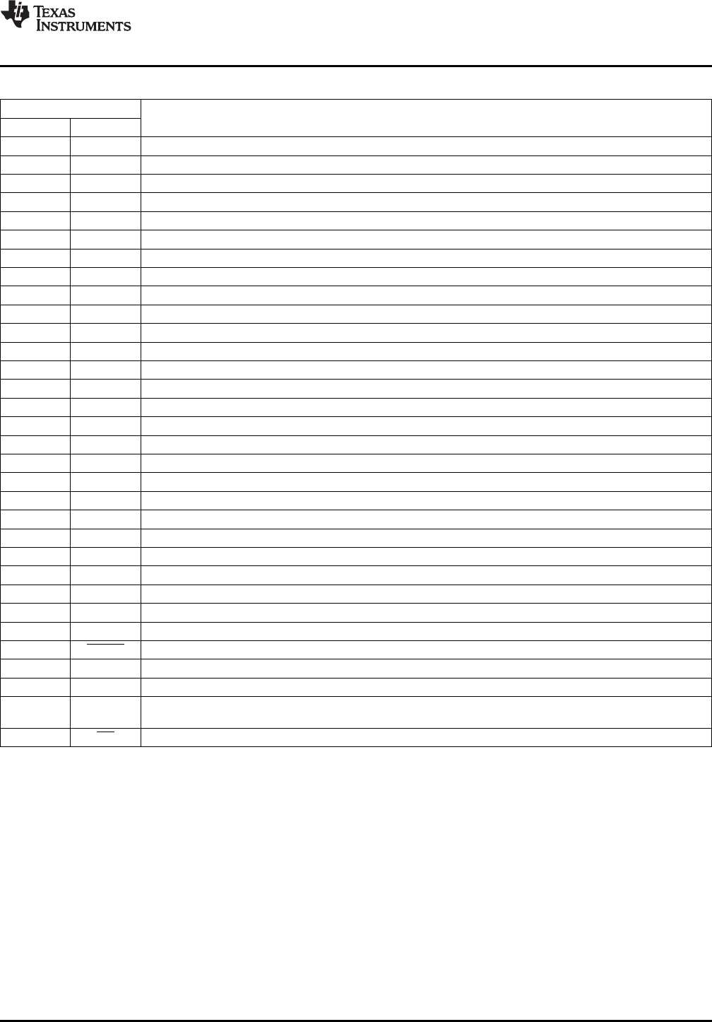
Table 1. TERMINAL FUNCTIONS
TERMINAL
DESCRIPTION
PIN NO. NAME
1 P00 P-port input/output (push-pull design structure). At power on, P00 is configured as an input.
2 P01 P-port input/output (push-pull design structure). At power on, P01 is configured as an input.
3 P02 P-port input/output (push-pull design structure). At power on, P02 is configured as an input.
4 P03 P-port input/output (push-pull design structure). At power on, P03 is configured as an input.
5 P04 P-port input/output (push-pull design structure). At power on, P04 is configured as an input.
6 P05 P-port input/output (push-pull design structure). At power on, P05 is configured as an input.
7 P06 P-port input/output (push-pull design structure). At power on, P06 is configured as an input.
8 P07 P-port input/output (push-pull design structure). At power on, P07 is configured as an input.
9 P10 P-port input/output (push-pull design structure). At power on, P10 is configured as an input.
10 P11 P-port input/output (push-pull design structure). At power on, P11 is configured as an input.
11 P12 P-port input/output (push-pull design structure). At power on, P12 is configured as an input.
12 P13 P-port input/output (push-pull design structure). At power on, P13 is configured as an input.
13 P14 P-port input/output (push-pull design structure). At power on, P14 is configured as an input.
14 P15 P-port input/output (push-pull design structure). At power on, P15 is configured as an input.
15 P16 P-port input/output (push-pull design structure). At power on, P16 is configured as an input.
16 P17 P-port input/output (push-pull design structure). At power on, P17 is configured as an input.
17 P20 P-port input/output (push-pull design structure). At power on, P20 is configured as an input.
18 P21 P-port input/output (push-pull design structure). At power on, P21 is configured as an input.
19 P22 P-port input/output (push-pull design structure). At power on, P22 is configured as an input.
20 P23 P-port input/output (push-pull design structure). At power on, P23 is configured as an input.
21 P24 P-port input/output (push-pull design structure). At power on, P24 is configured as an input.
22 P25 P-port input/output (push-pull design structure). At power on, P25 is configured as an input.
23 P26 P-port input/output (push-pull design structure). At power on, P26 is configured as an input.
24 P27 P-port input/output (push-pull design structure). At power on, P27 is configured as an input.
25 GND Ground
26 ADDR Address input. Connect directly to V
CCP
or ground.
27 V
CCP
Supply voltage of TCA6424A for P port
28 RESET Active-low reset input. Connect to V
CCI
through a pullup resistor, if no active connection is used.
29 SCL Serial clock bus. Connect to V
CCI
through a pullup resistor.
30 SDA Serial data bus. Connect to V
CCI
through a pullup resistor.
Supply voltage of I
2
C bus. Connect directly to the V
CC
of the external I
2
C master. Provides voltage-level
31 V
CCI
translation.
32 INT Interrupt output. Connect to V
CCI
through a pullup resistor.
Voltage Translation
Table 2 shows how to set up V
CC
levels for the necessary voltage translation between the I
2
C bus and the
TCA6424A.
Copyright © 2010, Texas Instruments Incorporated Submit Documentation Feedback 3
Product Folder Link(s): TCA6424A