
Incor User's Guide Digital Amplifier TAS5518


www.ti.com
2.2 PSU Control Interface (J902)
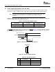
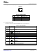
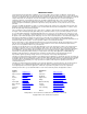
1
2
3
5
4
PCBConnector
(TopView)
PSU Control Interface (J902)
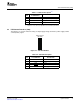
Table 2-3. J900 Pin Description
(1)
PIN NET NAME
DESCRIPTION
NO. AT SCHEMATICS
1 PVDD Extra output-stage power supply
2 PVDD Extras output-state power supply
3 GND Extra ground
4 GND Extra ground
(1)
Optional – Use to decrease impedance to reach better performance
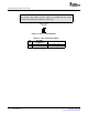
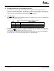
This interface is used for onboard sensing of output supply voltage and for the power supply volume
control (PSVC) signal.
Figure 2-3. J902 Pin Numbers
Table 2-4. J902 Pin Description
PIN NET NAME
DESCRIPTION
NO. AT SCHEMATICS
1 – Reserved for future use
2 PVDD Sense of output power supply
3 GND Ground
4 RESET System reset (bidirectional)
5 PSVC Power supply volume control
SLEU074 – June 2006 System Interfaces 13
Submit Documentation Feedback