
Digital Audio PWM Processor & Digital Amplifier User's Guide


www.ti.com
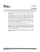
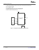
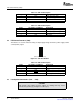
2.2 PSU Control Interface (J902)
1
2
3
5
4
(PCBconnectortopview)
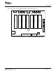
2.3 Loudspeaker Connectors (J101 … J107)
PSU Control Interface (J902)
Table 2-2. J901 Pin Description
PIN NO. NET-NAME AT SCHEMATICS DESCRIPTION
1 PVDD Output-stage power supply
2 SYSTEM System power supply
3 GND Ground
4 GND Ground
Table 2-3. J900 Pin Description
PIN NO. NET-NAME AT SCHEMATICS DESCRIPTION
1 PVDD Extra output-stage power supply
2 PVDD Extra output-stage power supply
3 GND Extra ground
4 GND Extra ground
This interface is used for onboard sensing of output supply voltage and for the power supply volume
control (PSVC) signal.
Figure 2-3. J902 Pin Numbers
Table 2-4. J902 Pin Description
PIN NO. NET-NAME AT SCHEMATICS DESCRIPTION
1 — Reserved for future use
2 PVDD Sense of output power supply
3 GND Ground
4 RESET System reset (bidirectional)
5 PSVC Power supply volume control signal
CAUTION
Both positive and negative speaker outputs are floating and may not be
connected to ground (e.g., through an oscilloscope).
System Interfaces10 SLEU071 – June 2006
Submit Documentation Feedback