
Datasheet


Table Of Contents
- 1 Overview
- 2 Quick Setup Guide
- 3 Protection
- 4 TAS5352DDV6EVM Performance
- 4.1 THD+N vs Power (BTL – 4 )
- 4.2 THD+N vs Power (BTL – 6 )
- 4.3 THD+N vs Power (BTL – 8 )
- 4.4 THD+N vs Power (PBTL – 2 )
- 4.5 THD+N vs Power (PBTL – 3 )
- 4.6 THD+N vs Frequency (BTL –4 )
- 4.7 THD+N vs Frequency (BTL –6 )
- 4.8 THD+N vs Frequency (BTL –8 )
- 4.9 THD+N vs Frequency (PBTL – 2 )
- 4.10 THD+N vs Frequency (PBTL – 3 )
- 4.11 FFT Spectrum With –60-dBFS Tone (BTL)
- 4.12 FFT Spectrum With –60-dBFS Tone (PBTL)
- 4.13 Idle Noise FFT Spectrum (BTL)
- 4.14 Idle Noise FFT Spectrum (PBTL)
- 4.15 Channel Separation
- 4.16 Frequency Response (BTL)
- 4.17 Frequency Response (PBTL)
- 4.18 High-Current Protection (BTL)
- 4.19 High-Current Protection (PBTL)
- 4.20 Pop/Click (BTL)
- 4.21 Pop/Click (PBTL)
- 4.22 Output Stage Efficiency
- 4.23 Subwoofer Lineout THD vs Output Voltage
- 4.24 Subwoofer Lineout THD+N vs Frequency
- 4.25 Subwoofer Lineout Frequency Response
- 5 Related Documentation from Texas Instruments
- Appendix A Design Documents
www.ti.com
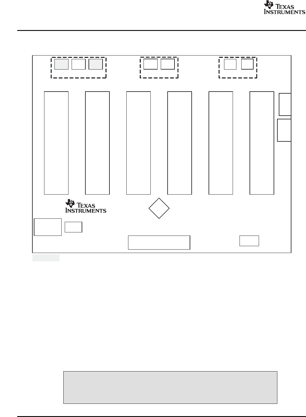
1.2 PCB Key Map
SPEAKEROUTPUTS
TAS5518
OUTPUT STAGE
CHANNEL 3
3.3V
Regulator
PSU
INTERFACE
(J901)
PSU
CONTROL
(J902)
INPUT SIGNAL& CONTROL
INTERFACE(J10)
SUBWOOFER
OUTPUT
(J600)
J101
BTL
J102
BTL
OUTPUT STAGE
CHANNEL 1
OUTPUT STAGE
CHANNEL 4
OUTPUT STAGE
CHANNEL 2
OUTPUT STAGE
CHANNEL 6
OUTPUT STAGE
CHANNEL 5
SPEAKEROUTPUTS
J103
BTL
J104
BTL
SPEAKEROUTPUTS
J117
PBTL
J107
BTL*
DRV600
J108
BTL*
*: ConfigOption
2 Quick Setup Guide
2.1 Electrostatic Discharge Warning
Quick Setup Guide
Physical structure for the TAS5352DDV6EVM is illustrated in Figure 2 .
Figure 2. Physical Structure for the TAS5352DDV6EVM (Approximate Layout)
This section describes the TAS5352DDV6EVM board in regards to power supplies and system interfaces.
The section provides information regarding handling and unpacking, absolute operating conditions, and a
description of the factory default switch and jumper configuration.
This section provides a step-by-step guide to configuring the TAS5352DDV6EVM for device evaluation.
Many of the components on the TAS5352DDV6EVM are susceptible to damage by electrostatic discharge
(ESD). Customers are advised to observe proper ESD handling precautions when unpacking and handling
the EVM, including the use of a grounded wrist strap at an approved ESD workstation.
CAUTION
Failure to observe ESD handling procedures may result in damage to EVM
components.
TAS5352DDV6EVM 6 SLAU244 – March 2008
Submit Documentation Feedback