
Datasheet


Table Of Contents
4 TAS5142DDV6EVM2 Performance
TAS5142DDV6EVM2 Performance
www.ti.com
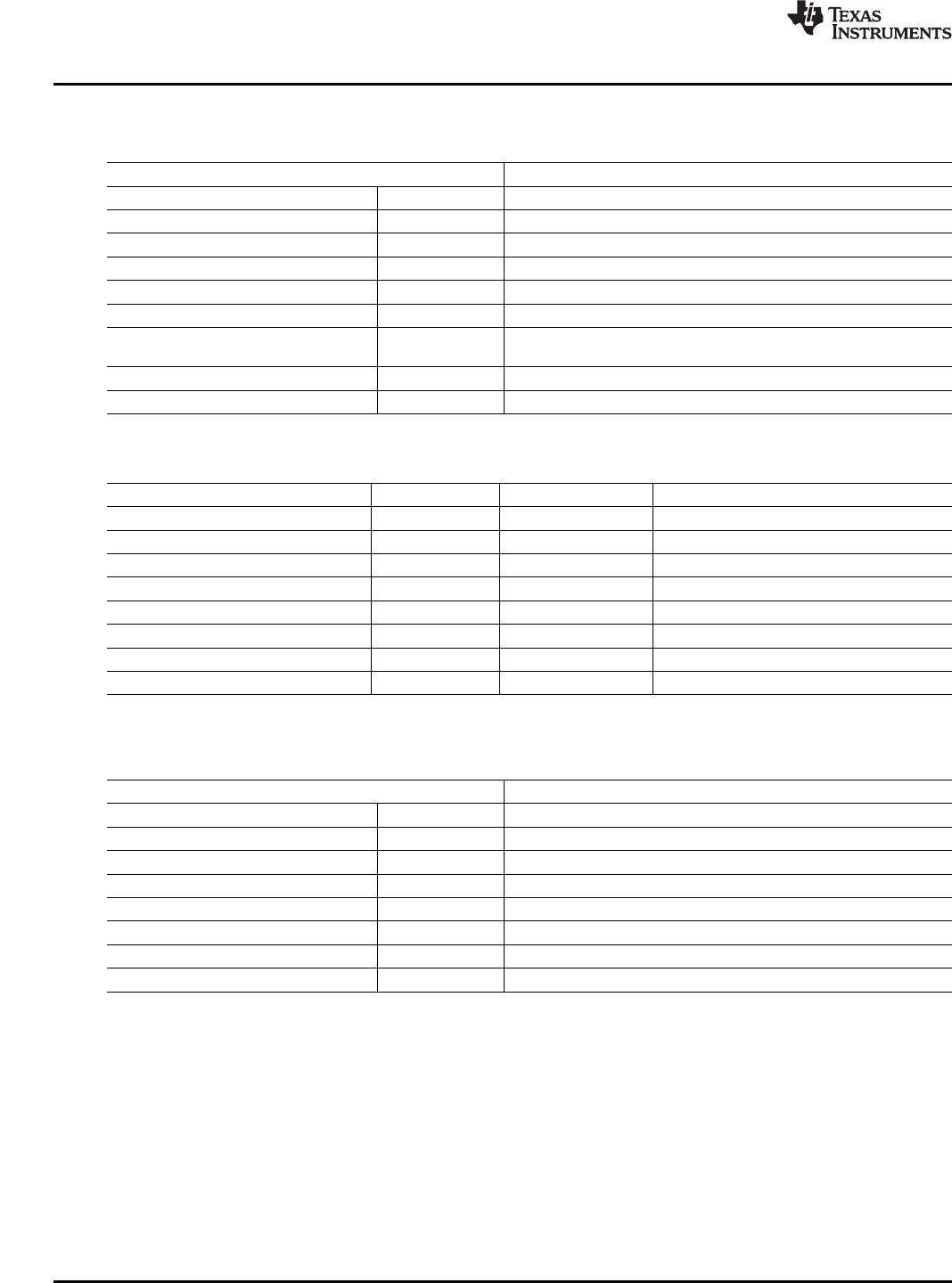
Table 4. General Test Conditions
General Test Conditions Notes
Output stage supply voltage 32 V Laboratory power supply (EA-PS 7065-10A)
System supply voltage 15 V
Load Impedance 4 Ω
Input signal 1-kHz sine
Sampling frequency 48 kHz
Gain setting in TAS5086 0 dB
AES17 and
Measurement filter
AUX-0025
TI input-USB board Input-USB Rev 9 S/N:898
EVM configuration file Ver 2.00 TAS5142DDV6EVM2 Configuration (2.00).cfg
Table 5. TAS5086 Register Settings
(1)
Register Name Register Number Value Notes
Oscillator trim register 0x1B 0x00 Initiate oscillator to factory trim
Master volume register 0x07 0x30 Set volume to 0 dB
Modulation limit register 0x10 0x04 Set maximum modulation to 96.1%
Split-capacitor charge period register 0x1A 0x00 No split-capacitor charge period
PWM start register 0x18 0x30
Input mux register 0x20 00 01 23 45
PWM mux register 0x25 00 01 23 45
System control register 0x05 0x20
(1)
These register settings are used for all tests, unless otherwise specified.
Table 6. Electrical Data
Electrical Data Notes/Conditions
Output power, 4 Ω 80 W 1 kHz, unclipped (0 dBFS), T
A
= 25 ° C
Output power, 4 Ω 100 W 1 kHz, 10% THD+N, T
A
= 25 ° C
Maximum peak current >10 A 1-kHz burst, 1 Ω , R
OC
= 22 k Ω
Output stage efficiency 83% 1 kHz, 2 × 100 W, 4 Ω
Damping factor 12 1 kHz, relative to 8- Ω load
System supply current <200 mA 1-kHz, –60-dBFS signal, with TI input board
H-bridge supply current <250 mA 1-kHz, –60-dBFS signal
Total board idle power consumption 11 W H-bridge supply + system supply, –60-dBFS signal
TAS5142DDV6EVM2 10 SLLU095A – April 2007 – Revised April 2008
Submit Documentation Feedback