
Datasheet


VIO
10kW
Tothe outputsforINT
additionalSRC4392 devices
Interrupt
Logic
SRC4392 MCU,DSP,
orLogic
INT
23
Interrupt
Input
S A A A A A P
Byte1
Slav Ade dress
wit Rh /W=0
Byte2
Reg tis erAddressByte
wit Ih NC=1
Byte3
SlaveAddress
withR/W=1
Byte4
Reg tis erData
ByteN
Reg tis erData
ForAddress+N
(c)RandomReadOp mentEnablederation,Auto-Incre
S=STARTC dion tion
A=Ackn w dgo le e
A =NotAckno ledgew
R=Repeated TARTS
P=STOPCondii nt o
Transferfrom steMa r to Slave
Transferfrom avetoSl Master
L gende
R
S A A P
Byte1
SlaveAddre ss
withR/W=1
Byte2
Reg tis erAddressByte
withINC=0
(a Cu) rrentAd res heRegister ddr ss fthe vio sd A e Pre us Read,Assumest o
S A A
A P
Byte1
Slav Ade dress
withR/W=0
Byte2
Reg tis erAddressByte
withINC=0
Byte3
Slav Ade dress
withR/W=1
(b)RandomReadOp me tDisablederation,Auto-Incre n
R
A
Byte4
RegisterData
SRC4392
www.ti.com
SBFS029D –DECEMBER 2005–REVISED DECEMBER 2012
Figure 78. Fast/Standard Mode Read Operations
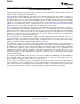
INTERRUPT OUTPUT
The SRC4392 includes multiple internal status bits, many of which may be set to trigger an interrupt signal. The
interrupt signal is output at INT (pin 23), which is an active low, open-drain output. The INT pin requires a pull-up
resistor to the VIO supply rail. The value of the pull-up is not critical, but a 10kΩ device should be sufficient for
most applications. Figure 79 shows the interrupt output pin connection. The open-drain output allows interrupt
pins from multiple SRC4392 devices to be connected in a wired OR configuration.
Figure 79. Interrupt Output Pin Connections
Copyright © 2005–2012, Texas Instruments Incorporated Submit Documentation Feedback 39
Product Folder Links: SRC4392