
Datasheet


CS
CDNI
CC KL
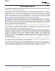
Set =1hereto gisterlocation.write/readonereCS
Hold =0toenab de.leauto-incrementmoCS
Byte0 Byte1 Byte2 Byte3
ByteN
R/W A6 A5 A0A4 A1A3 A2
Setto 0forWrite ad.; Setto orRe1f
Byte0:
MSB LSB
ByteDefi itionn
Header
RegisterData
RegisterAddress
Byte1:DontCar’ e
Byte2 throughByteN: RegisterD ta a
CDOUT
HiZ HiZ DataforA[ : ]+16 0DataforA[6:0]
DataforA[ : ]+N2 0
RegisterData
SRC4392
www.ti.com
SBFS029D –DECEMBER 2005–REVISED DECEMBER 2012
Refer to the Electrical Characteristics: SPI Interface table and Figure 2 for specifications and a timing diagram
that highlight the key parameters for SPI interface operation.
Figure 75. Serial Peripheral Interface (SPI) Protocol for the SRC4392
HOST INTERFACE OPERATION: PHILIPS I
2
C MODE
The SRC4392 supports a 2-wire Philips I
2
C bus interface when CPM (pin 18) is forced high or pulled up to the
VIO supply rail. The SRC4392 functions as a Slave-only device on the bus. Standard and Fast modes of
operation are supported. Standard mode supports data rates up to 100kbps, while Fast mode supports data
rates up to 400kbps. Fast mode is downward compatible with Standard mode, and these modes are sometimes
referred to as Fast/Standard, or F/S mode. The I
2
C Bus Specification (Version 2.1, January 2000), available from
Philips Semiconductor, provides the details for the bus protocol and implementation. It is assumed that the
reader is familiar with this specification. Refer to the Electrical Characteristics: I
2
C Standard and Fast Modes
table and Figure 3 for specifications and a timing diagram that highlight the key parameters for I
2
C interface
operation.
When the I
2
C mode is invoked, pin 20 becomes SCL (which serves as the bus clock) and pin 22 becomes SDA
(which carries the bi-directional serial data for the bus). Pins 19 and 21 become A0 and A1, respectively, and
function as the hardware configurable portion of the 7-bit slave address.
The SRC4392 utilizes a 7-bit Slave address, see Figure 76(a). Bits A2 through A6 are fixed and bits A0 and A1
are hardware programmable using pins 19 and 21, respectively. The programmable bits allow for up to four
SRC4392 devices to be connected to the same bus. The slave address is followed by the Register Address Byte,
which points to a specific register or data buffer location in the SRC4392 register map. The register address byte
is comprised of seven bits for the address, and one bit for enabling or disabling auto-increment operation, see
Figure 76(b). Auto-increment mode allows multiple sequential register locations to be written to or read back in a
single operation, and is especially useful for block write and read operations.
Figure 77 illustrates the protocol for Standard and Fast mode Write operations. When writing a single register
address, or multiple non-sequential register addresses, the single register write operation of Figure 77(a) may be
used one or more times. When writing multiple sequential register addresses, the auto-increment mode of
Figure 77(b) improves efficiency. The register address is automatically incremented by one for each successive
byte of data transferred.
Figure 78 illustrates the protocol for Standard and Fast mode Read operations. The current address read
operation of Figure 78(a) assumes the value of the register address from the previously executed write or read
operation, and is useful for polling a register address for status changes. Figure 78(b) and Figure 78(c) illustrate
read operations for one or more random register addresses, with or without auto-increment mode enabled.
Copyright © 2005–2012, Texas Instruments Incorporated Submit Documentation Feedback 37
Product Folder Links: SRC4392