SRC4392 www.ti.
SRC4392 SBFS029D – DECEMBER 2005 – REVISED DECEMBER 2012 APPLICATIONS • • • • • • • DIGITAL AUDIO RECORDERS AND MIXING DESKS DIGITAL AUDIO INTERFACES FOR COMPUTERS DIGITAL AUDIO ROUTERS AND DISTRIBUTION SYSTEMS BROADCAST STUDIO EQUIPMENT DVD/CD RECORDERS SURROUND SOUND DECODERS AND A/V RECEIVERS CAR AUDIO SYSTEMS DESCRIPTION The SRC4392 is a highly-integrated CMOS device designed for use in professional and broadcast digital audio systems.
SRC4392 www.ti.com SBFS029D – DECEMBER 2005 – REVISED DECEMBER 2012 This integrated circuit can be damaged by ESD. Texas Instruments recommends that all integrated circuits be handled with appropriate precautions. Failure to observe proper handling and installation procedures can cause damage. ESD damage can range from subtle performance degradation to complete device failure.
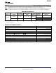
SRC4392 SBFS029D – DECEMBER 2005 – REVISED DECEMBER 2012 www.ti.com ELECTRICAL CHARACTERISTICS: General, SRC, DIR, and DIT All specifications are at TA = +25°C, VDD18 = +1.8V, VDD33 = +3.3V, VIO = +3.3V, and VCC = +3.3V, unless otherwise noted. SRC4392 PARAMETER CONDITIONS MIN TYP MAX UNITS V DIGITAL I/O CHARACTERISTICS (All I/O Pins Except Line Receivers and Line Driver) High-Level Input Voltage, VIH 0.7 × VIO VIO Low-Level Input Voltage, VIL 0 0.
SRC4392 www.ti.com SBFS029D – DECEMBER 2005 – REVISED DECEMBER 2012 ELECTRICAL CHARACTERISTICS: General, SRC, DIR, and DIT (continued) All specifications are at TA = +25°C, VDD18 = +1.8V, VDD33 = +3.3V, VIO = +3.3V, and VCC = +3.3V, unless otherwise noted. SRC4392 PARAMETER Total Harmonic Distortion + Noise (THD+N) (2) CONDITIONS MIN TYP MAX UNITS BW = 22Hz to fSOUT/2, f = 997Hz at 0dBFS fSIN:fSOUT = 12kHz:192kHz –137 dB fSIN:fSOUT = 44.1kHz:44.1kHz –140 dB fSIN:fSOUT = 44.
SRC4392 SBFS029D – DECEMBER 2005 – REVISED DECEMBER 2012 www.ti.com ELECTRICAL CHARACTERISTICS: General, SRC, DIR, and DIT (continued) All specifications are at TA = +25°C, VDD18 = +1.8V, VDD33 = +3.3V, VIO = +3.3V, and VCC = +3.3V, unless otherwise noted. SRC4392 PARAMETER CONDITIONS MIN TYP MAX UNITS DIGITAL AUDIO INTERFACE RECEIVER (DIR) PLL Lock Range 20 216 kHz Reference Clock Input (RXCKI) Frequency, fRXCKI 3.5 27.
SRC4392 www.ti.com SBFS029D – DECEMBER 2005 – REVISED DECEMBER 2012 ELECTRICAL CHARACTERISTICS: I2C Standard and Fast Modes All specifications are at TA = +25°C, VDD18 = +1.8V, VDD33 = +3.3V, VIO = +3.3V, and VCC = +3.3V, unless otherwise noted. SRC4392 PARAMETER CONDITIONS MIN TYP MAX UNITS 100 kHz HOST INTERFACE: I2C Standard Mode (1) SCL Clock Frequency, fSCL 0 Hold Time Repeated START Condition, tHDSTA 4 μs Low Period of SCL Clock, tLOW 4.
SRC4392 SBFS029D – DECEMBER 2005 – REVISED DECEMBER 2012 www.ti.com ELECTRICAL CHARACTERISTICS: Power Supplies All specifications are at TA = +25°C, VDD18 = +1.8V, VDD33 = +3.3V, VIO = +3.3V, and VCC = +3.3V, unless otherwise noted. SRC4392 PARAMETER CONDITIONS MIN TYP MAX UNITS VDD18 +1.65 +1.8 +1.95 V VDD33 +3.0 +3.3 +3.6 V VIO +1.65 +3.3 +3.6 V VCC +3.0 +3.3 +3.
SRC4392 www.ti.com SBFS029D – DECEMBER 2005 – REVISED DECEMBER 2012 TIMING DIAGRAMS LRCK tBCKH BCK tBCKL tAIS SDIN tAIH tAOD SDOUT Figure 1. Audio Serial Port Timing tCFCS CS tCSCR tCDS CCLK tCDH CDIN Hi Z Hi Z CDOUT tCFDO tCSZ Figure 2. SPI Interface Timing tF SDA tLOW tSUDAT tR tHDSTA tSP tR tBUF tF SCL tHDSTA S tSUSTA tHDDAT tHIGH S = Start Condition tSUSTO R P R = Repeated Start Condition P = Stop Condition S Figure 3.
SRC4392 SBFS029D – DECEMBER 2005 – REVISED DECEMBER 2012 www.ti.
SRC4392 www.ti.com SBFS029D – DECEMBER 2005 – REVISED DECEMBER 2012 PIN DESCRIPTIONS (continued) PIN NO.
SRC4392 SBFS029D – DECEMBER 2005 – REVISED DECEMBER 2012 www.ti.com TYPICAL CHARACTERISTICS All specifications are at TA = +25°C, VDD18 = +1.8V, VDD33 = +3.3V, VIO = +3.3V, and VCC = +3.3V, unless otherwise noted. THD+N vs INPUT SAMPLING RATE (fSOUT = 48kHz and fIN = 997Hz at 0dBFS) -130 -130 -132 -132 -134 -134 -136 -136 THD+N (dB) -138 -140 -142 -138 -140 -142 -144 -144 -146 -146 -148 -148 -150 -150 32 52 72 92 112 132 152 172 32 192 52 72 132 152 172 Figure 5.
SRC4392 www.ti.com SBFS029D – DECEMBER 2005 – REVISED DECEMBER 2012 TYPICAL CHARACTERISTICS (continued) All specifications are at TA = +25°C, VDD18 = +1.8V, VDD33 = +3.3V, VIO = +3.3V, and VCC = +3.3V, unless otherwise noted.
SRC4392 SBFS029D – DECEMBER 2005 – REVISED DECEMBER 2012 www.ti.com TYPICAL CHARACTERISTICS (continued) All specifications are at TA = +25°C, VDD18 = +1.8V, VDD33 = +3.3V, VIO = +3.3V, and VCC = +3.3V, unless otherwise noted.
SRC4392 www.ti.com SBFS029D – DECEMBER 2005 – REVISED DECEMBER 2012 TYPICAL CHARACTERISTICS (continued) All specifications are at TA = +25°C, VDD18 = +1.8V, VDD33 = +3.3V, VIO = +3.3V, and VCC = +3.3V, unless otherwise noted.
SRC4392 SBFS029D – DECEMBER 2005 – REVISED DECEMBER 2012 www.ti.com TYPICAL CHARACTERISTICS (continued) All specifications are at TA = +25°C, VDD18 = +1.8V, VDD33 = +3.3V, VIO = +3.3V, and VCC = +3.3V, unless otherwise noted. FFT PLOT (fSIN:fSOUT = 44.1kHz:48kHz and Input Frequency = 997Hz at 0dBFS) 0 0 -20 -20 -40 -40 -60 -60 Amplitude (dB) Amplitude (dB) FFT PLOT (fSIN:fSOUT = 44.1kHz:44.
SRC4392 www.ti.com SBFS029D – DECEMBER 2005 – REVISED DECEMBER 2012 TYPICAL CHARACTERISTICS (continued) All specifications are at TA = +25°C, VDD18 = +1.8V, VDD33 = +3.3V, VIO = +3.3V, and VCC = +3.3V, unless otherwise noted.
SRC4392 SBFS029D – DECEMBER 2005 – REVISED DECEMBER 2012 www.ti.com TYPICAL CHARACTERISTICS (continued) All specifications are at TA = +25°C, VDD18 = +1.8V, VDD33 = +3.3V, VIO = +3.3V, and VCC = +3.3V, unless otherwise noted. FFT PLOT (fSIN:fSOUT = 192kHz:48kHz and Input Frequency = 997Hz at 0dBFS) 0 0 -20 -20 -40 -40 -60 -60 Amplitude (dB) Amplitude (dB) FFT PLOT (fSIN:fSOUT = 192kHz:44.
SRC4392 www.ti.com SBFS029D – DECEMBER 2005 – REVISED DECEMBER 2012 TYPICAL CHARACTERISTICS (continued) All specifications are at TA = +25°C, VDD18 = +1.8V, VDD33 = +3.3V, VIO = +3.3V, and VCC = +3.3V, unless otherwise noted. IMD (fSIN:fSOUT = 96kHz:48kHz, SMPTE/DIN 1:1, 10kHz and 11kHz, and –0.1dB Input Amplitude) 0 -20 Amplitude (dB) -40 -60 -80 -100 -120 -140 -160 -180 -200 0 2 4 6 8 10 12 14 16 18 20 22 24 Frequency (kHz) Figure 58.
SRC4392 SBFS029D – DECEMBER 2005 – REVISED DECEMBER 2012 www.ti.com PRODUCT OVERVIEW The SRC4392 is a two-channel asynchronous sample rate converter (SRC) with an integrated digital audio interface receiver and transmitter (DIR and DIT). Two audio serial ports, Port A and Port B, support input and output interfacing to external data converters, signal processors, and logic devices. On-chip routing logic provides for flexible interconnection between the five functional blocks.
SRC4392 www.ti.com SBFS029D – DECEMBER 2005 – REVISED DECEMBER 2012 Figure 59 shows a simplified functional block diagram for the SRC4392. Additional details for each function block will be covered in respective sections of this datasheet.
SRC4392 SBFS029D – DECEMBER 2005 – REVISED DECEMBER 2012 www.ti.com Write or Read via 2 SPI or I C 1 RST 0 500ns (min) 500ms (min) Figure 60. Reset Sequence Timing MASTER AND REFERENCE CLOCKS The SRC4392 includes two clock inputs, MCLK (pin 25) and RXCKI (pin 13). The MCLK clock input is typically used as the master clock source for the audio serial ports, the DIT, and/or the SRC. The MCLK may also be utilized as the reference clock for the DIR.
SRC4392 www.ti.com SBFS029D – DECEMBER 2005 – REVISED DECEMBER 2012 AUDIO SERIAL PORT OPERATION The SRC4392 includes two audio serial ports, Port A and Port B. Both ports are 4-wire synchronous serial interfaces, supporting simultaneous input and output operation. Since each port has only one pair of left/right word and bit clocks, the input and output sampling rates are identical. A simplified block diagram is shown in Figure 61.
SRC4392 SBFS029D – DECEMBER 2005 – REVISED DECEMBER 2012 www.ti.com Channel 1 (Left Channel) Channel 2 (Right Channel) LRCKA LRCKB BCKA BCKB Audio Data MSB LSB MSB LSB (a) Left-Justified Data Format LRCKA LRCKB BCKA BCKB Audio MSB Data LSB MSB LSB (b) Right-Justified Data Format LRCKA LRCKB BCKA BCKB Audio Data MSB LSB MSB LSB 2 (c) I S Data Format 1/fs Figure 62.
SRC4392 www.ti.com SBFS029D – DECEMBER 2005 – REVISED DECEMBER 2012 For AES3 transmission, data is encoded into frames, with each frame containing two subframes of audio and status data, corresponding to audio Channels 1 and 2 (or Left and Right, respectively, for stereophonic audio). Figure 63 shows the AES3 frame and subframe formatting.
SRC4392 SBFS029D – DECEMBER 2005 – REVISED DECEMBER 2012 www.ti.com The binary non-return to zero (NRZ) formatted audio and status source data for bits 4 through 31 of each subframe are encoded utilizing a Biphase Mark format for transmission. This format allows for clock recovery at the receiver end, as well as making the interface insensitive to the polarity of the balanced cable connections.
SRC4392 www.ti.com SBFS029D – DECEMBER 2005 – REVISED DECEMBER 2012 The AES3 encoder output is connected to the output line driver and CMOS buffer source multiplexers. As shown in Figure 65, the source multiplexers allow the line driver or buffer to be driven by the AES3-encoded data from the DIT, or by the bypass multiplexer, which is associated with the outputs of the four differential input line receivers preceding the DIR core.
SRC4392 SBFS029D – DECEMBER 2005 – REVISED DECEMBER 2012 www.ti.com Block Start (Frame 0 starts here) SYNC BLS (input) BLS (output) Figure 66. DIT Block Start Timing DIGITAL INTERFACE RECEIVER (DIR) OPERATION The DIR performs AES3 decoding and clock recovery and provides the differential line receiver functions. The lock range of the DIR includes frame/sampling rates from 20kHz to 216kHz. Figure 67 shows the functional block diagram for the DIR.
SRC4392 www.ti.com SBFS029D – DECEMBER 2005 – REVISED DECEMBER 2012 VDD33 24kW 24kW 3kW RX+ To Receiver Input and Bypass Multiplexers RX3kW 24kW 24kW DGND2 Figure 68. Differential Line Receiver Circuit The outputs of the four line receivers are connected to two 1-of-4 data selectors: the receiver input multiplexer and the bypass multiplexer. The input multiplexer selects one of the four line receiver outputs as the source for the AES3-encoded data stream to be processed by the DIR core.
SRC4392 SBFS029D – DECEMBER 2005 – REVISED DECEMBER 2012 www.ti.com 2 0 Jitter Attenuation (dB) -2 -4 -6 -8 -10 -12 -14 -16 -18 -20 10 0 10 1 10 2 10 3 10 4 10 5 10 6 Jitter Frequency (Hz) -10 -20 -30 -40 -50 -60 -70 -80 -90 -100 -110 -120 -130 -140 -150 5 2 Input Jitter Amplitude 1 Output Jitter Amplitude 500m 200m Peak Jitter (UI) THD+N Ratio (dB) Figure 69.
SRC4392 www.ti.com SBFS029D – DECEMBER 2005 – REVISED DECEMBER 2012 ASYNCHRONOUS SAMPLE RATE CONVERTER (SRC) OPERATION The asynchronous SRC provides conversion from an arbitrary input sampling rate to a desired output sampling rate. The input and output sampling rates may be equal or different, within the bounds of a 1:16 to 16:1 input-tooutput sampling ratio range. The input and output data sources may be completely asynchronous to one another; synchronous operation is also supported.
SRC4392 SBFS029D – DECEMBER 2005 – REVISED DECEMBER 2012 www.ti.com The input and output servo-loop frequency responses are shown in Figure 73 and Figure 74, respectively. The filter response for each servo loop rolls off at 80dB per decade. The servo loop corner frequencies scale proportionally with input or output sampling rates. The low corner frequency and sharp roll-off provide excellent jitter attenuation for the SRC block.
SRC4392 www.ti.com SBFS029D – DECEMBER 2005 – REVISED DECEMBER 2012 DEM0 and DEM1 bits. The AUTODEM function automatically enables and disables the de-emphasis filter for the required sampling rate based upon the setting of the pre-emphasis and sampling frequency channel status bits in the AES3 or S/PDIF input data stream, which are decoded by the DIR block. The AUTODEM feature functions only when both 50/15μs pre-emphasis and one of the three supported sampling rates (32kHz, 44.
SRC4392 SBFS029D – DECEMBER 2005 – REVISED DECEMBER 2012 www.ti.com GENERAL-PURPOSE DIGITAL OUTPUTS The SRC4392 includes four general-purpose digital outputs, GPO1 through GPO4 (pins 26 through 29, respectively). A GPO pin may be programmed to a static high or low state. Alternatively, a GPO pin may be connected to one of 14 internal logic nodes, allowing the GPO pin to inherit the function of the selected signal. Control registers 0x1B through 0x1E are utilized to select the function of the GPO pins.
SRC4392 www.ti.com SBFS029D – DECEMBER 2005 – REVISED DECEMBER 2012 Refer to the Electrical Characteristics: SPI Interface table and Figure 2 for specifications and a timing diagram that highlight the key parameters for SPI interface operation. Set CS = 1 here to write/read one register location. Hold CS = 0 to enable auto-increment mode.
SRC4392 SBFS029D – DECEMBER 2005 – REVISED DECEMBER 2012 www.ti.com First Byte After the START/RESTART Condition Slave Address LSB MSB A6 A5 A4 A3 A2 A1 A0 1 1 1 0 0 A1 A0 R/W Set by Pin 19 Set by Pin 21 (a) SRC4392 Slave Address MSB LSB INC A6 Auto-Increment 0 = Disabled 1 = Enabled A5 A4 A3 A2 A1 A0 (b) Register Address Byte Figure 76.
SRC4392 www.ti.
SRC4392 SBFS029D – DECEMBER 2005 – REVISED DECEMBER 2012 www.ti.com APPLICATIONS INFORMATION Typical application diagrams and power-supply connections are presented in this section to aid the customer in hardware designs employing the SRC4392 device. Figure 80 illustrates typical application connections for the SRC4392 using an SPI host interface. The SPI host will typically be a microcontroller, digital signal processor, or a programmable logic device.
SRC4392 www.ti.
SRC4392 SBFS029D – DECEMBER 2005 – REVISED DECEMBER 2012 www.ti.com +3.3V 10mF + 44 R 0.1mF 43 42 SRC4392IPFB 9 10mF + 33 0.1mF 0.1mF 10 + 10mF 30 Connect pin 44 to pin 10. Pin 10 is then connected to the ground plane. +3.3V TPS79318DBVR 1 IN 3 EN 0.1mF GND 2 OUT NR 16 17 0.1mF 5 4 C 0.01mF 2.2mF + +1.8V Optional Regulator Circuit R may be set from 2W to 10W, or replaced by a ferrite bead. C may be set to 10mF, or not installed when using the optional regulator circuit.
SRC4392 www.ti.com SBFS029D – DECEMBER 2005 – REVISED DECEMBER 2012 RECEIVER INPUT INTERFACING This section details the recommended interfaces for the SRC4392 line receiver inputs. Balanced and unbalanced line interfaces, in addition to optical receiver and external logic interfacing, will be discussed. For professional digital audio interfaces, 110Ω balanced line interfaces are either required or preferred.
SRC4392 SBFS029D – DECEMBER 2005 – REVISED DECEMBER 2012 www.ti.com Optical interfaces utilizing all-plastic fiber are commonly employed for consumer audio equipment where interconnections are less than 10m in length. Optical receiver modules utilized for a digital audio interface operate from either a single +3.3V or +5V supply and have a TTL-, CMOS-, or low-voltage CMOS-compatible logic output. Interfacing to +3.
SRC4392 www.ti.com SBFS029D – DECEMBER 2005 – REVISED DECEMBER 2012 The SRC4392 line receivers may also be driven directly from external logic or line receiver devices with TTL or CMOS outputs. If the logic driving the line receiver is operated from +3.3V, then logic level translation is not be required. However, if the external logic is operated from a power-supply voltage that exceeds the maximum VDD33 supply voltage of the SRC4392, or operates from a supply voltage lower than +3.
SRC4392 SBFS029D – DECEMBER 2005 – REVISED DECEMBER 2012 0.1mF www.ti.com 1:1 R1 TX+ Digital Output 75W Unbalanced (RCA or BNC connector) R2 (a) Transformer-Coupled Unbalanced Output 0.1mF R1 TX+ Digital Output 75W Unbalanced (RCA or BNC connector) R2 (b) Unbalanced Output Without Transformer R1 and R2 are selected to achieve the desired output voltage level while maintaining the required 75W transmitter output impedance. The TX+ output impedance is negligible. Figure 89.
SRC4392 www.ti.com SBFS029D – DECEMBER 2005 – REVISED DECEMBER 2012 Direct to external logic operating from the VIO supply. AESOUT +5V 5 2 4 3 To +5V Logic (VIO supply = +3.0V to +3.3V) 1 SN74AHCT1G125 or Equivalent Figure 91. CMOS/TTL Output Logic Interface +5V SN75ALS191 1 8 2 AESOUT 7 VIO 1 +3.3V 5 6 3 6 If VIO < +3.0V. 4 3 5 SN74AVC1T45 or Equivalent To Balanced or Unbalanced Line Interface To Balanced or Unbalanced Line Interface 2 1 Figure 92.
SRC4392 SBFS029D – DECEMBER 2005 – REVISED DECEMBER 2012 www.ti.com REGISTER AND DATA BUFFER ORGANIZATION The SRC4392 organizes the on-chip registers and data buffers into four pages. The currently active page is chosen by programming the Page Selection Register to the desired page number. The Page Selection Register is available on every register page at address 0x7F, allowing easy movement between pages. Table 2 indicates the page selection corresponding to the Page Selection Register value. Table 2.
SRC4392 www.ti.com SBFS029D – DECEMBER 2005 – REVISED DECEMBER 2012 Table 3.
SRC4392 SBFS029D – DECEMBER 2005 – REVISED DECEMBER 2012 www.ti.com Register 01: Power-Down and Reset Bit 7 (MSB) Bit 6 Bit 5 Bit 4 Bit 3 Bit 2 Bit 1 Bit 0 (LSB) RESET 0 PDALL PDPA PDPB PDTX PDRX PDSRC PDSRC Power-Down for the SRC Function Block This bit is utilized to power-down the SRC and associated functions. PDSRC PDRX SRC Power-Down Mode 0 Enabled (Default) 1 Disabled; the SRC function block will operate normally based upon the applicable control register settings.
SRC4392 www.ti.com PDSRC SBFS029D – DECEMBER 2005 – REVISED DECEMBER 2012 Power-Down for the SRC Function Block Disabled; all function blocks will operate normally based upon the applicable control register settings. 1 RESET Software Reset This bit is used to force a reset initialization sequence, and is equivalent to forcing an external reset via the RST input (pin 24). RESET Reset Function 0 Disabled (Default) 1 Enabled; all control registers will be reset to the default state.
SRC4392 SBFS029D – DECEMBER 2005 – REVISED DECEMBER 2012 www.ti.com Register 03: Port A Control Register 1 Bit 7 (MSB) Bit 6 Bit 5 Bit 4 Bit 3 Bit 2 Bit 1 Bit 0 (LSB) 0 AMUTE AOUTS1 AOUTS0 AM/S AFMT2 AFMT1 AFMT0 AFMT[2:0] Port A Audio Data Format These bits are used to set the audio input and output data format for Port A. Refer to the Audio Serial Port Operation section for illustrations of the supported data formats.
SRC4392 www.ti.com SBFS029D – DECEMBER 2005 – REVISED DECEMBER 2012 Register 04: Port A Control Register 2 Bit 7 (MSB) Bit 6 Bit 5 Bit 4 Bit 3 Bit 2 Bit 1 Bit 0 (LSB) 0 0 0 0 ACLK1 ACLK0 ADIV1 ADIV0 ADIV[1:0] Port A Master Clock Divider These bits are used to set the master clock divider for generating the LRCKA clock for Port A when configured for Master mode operation. BCKA is always set to 64 times the LRCKA clock rate in Master mode.
SRC4392 SBFS029D – DECEMBER 2005 – REVISED DECEMBER 2012 www.ti.com Register 05: Port B Control Register 1 Bit 7 (MSB) Bit 6 Bit 5 Bit 4 Bit 3 Bit 2 Bit 1 Bit 0 (LSB) 0 BMUTE BOUTS1 BOUTS0 BM/S BFMT2 BFMT1 BFMT0 BFMT[2:0] Port B Audio Data Format These bits are used to set the audio input and output data format for Port B. Refer to the Audio Serial Port Operation section for illustrations of the supported data formats.
SRC4392 www.ti.com SBFS029D – DECEMBER 2005 – REVISED DECEMBER 2012 Register 06: Port B Control Register 2 Bit 7 (MSB) Bit 6 Bit 5 Bit 4 Bit 3 Bit 2 Bit 1 Bit 0 (LSB) 0 0 0 0 BCLK1 BCLK0 BDIV1 BDIV0 BDIV[1:0] Port B Master Mode Clock Divider These bits are used to set the master clock divider for generating the LRCKB clock for Port B when configured for Master mode operation. BCKB is always set to 64 times the LRCKB clock rate in Master mode.
SRC4392 SBFS029D – DECEMBER 2005 – REVISED DECEMBER 2012 BLSM www.ti.com Transmitter Block Start Input/Output Mode This bit is used to select the input/output mode for the DIT block start pin, BLS (pin 35). TXIS[1:0] BLSM BLS Pin Mode 0 Input (Default) 1 Output Transmitter Input Data Source These bits are used to select the audio data source for the DIT function block.
SRC4392 www.ti.com AESOFF SBFS029D – DECEMBER 2005 – REVISED DECEMBER 2012 AESOUT Output Enable This bit is used to enable or disable the AESOUT (pin 34) buffered AES3-encoded CMOS logic level output. AESOFF TXBTD AESOUT Output 0 Enabled; the AESOUT pin functions normally. (Default) 1 Disabled; the AESOUT pin is forced low.
SRC4392 SBFS029D – DECEMBER 2005 – REVISED DECEMBER 2012 www.ti.com Register 09: Transmitter Control Register 3 Bit 7 (MSB) Bit 6 Bit 5 Bit 4 Bit 3 Bit 2 Bit 1 Bit 0 (LSB) 0 0 0 0 0 VALSEL TXCUS1 TXCUS0 TXCUS[1:0] Transmitter Channel Status and User Data Source These bits select the source of the channel status (or C) data and user (or U) data which is used to load the DIT User Access (UA) buffers. TXCUS1 TXCUS0 0 0 The buffers will not be updated.
SRC4392 www.ti.
SRC4392 SBFS029D – DECEMBER 2005 – REVISED DECEMBER 2012 www.ti.com Register 0B: SRC and DIT Interrupt Mask Register Bit 7 (MSB) Bit 6 Bit 5 Bit 4 Bit 3 Bit 2 Bit 1 Bit 0 (LSB) 0 0 MRATIO MREADY 0 0 MTSLIP MTBTI MBTI Transmitter Buffer Transfer Interrupt Mask MTBI MTSLIP BTI Interrupt Mask 0 BTI interrupt is masked. (Default) 1 BTI interrupt is enabled. Transmitter TSLIP Interrupt Mask MTSLIP MREADY TSLIP Interrupt Mask 0 TSLIP interrupt is masked.
SRC4392 www.ti.com SBFS029D – DECEMBER 2005 – REVISED DECEMBER 2012 Register 0C: SRC and DIT Interrupt Mode Register Bit 7 (MSB) Bit 6 Bit 5 Bit 4 Bit 3 Bit 2 Bit 1 Bit 0 (LSB) RATIOM1 RATIOM0 READYM1 READYM0 TSLIPM1 TSLIPM0 TBTIM1 TBTIM0 TBTIM[1:0] Transmitter Buffer Transfer Interrupt Mode These bits are utilized to select the active trigger state for the BTI interrupt.
SRC4392 SBFS029D – DECEMBER 2005 – REVISED DECEMBER 2012 www.ti.com Register 0D: Receiver Control Register 1 Bit 7 (MSB) Bit 6 Bit 5 Bit 4 Bit 3 Bit 2 Bit 1 Bit 0 (LSB) 0 0 0 RXBTD RXCLK 0 RXMUX1 RXMUX0 RXMUX[1:0] Receiver Input Source Selection These bits are used to select the output of the line receiver to be used as the input data source for the DIR core.
SRC4392 www.ti.com SBFS029D – DECEMBER 2005 – REVISED DECEMBER 2012 Register 0E: Receiver Control Register 2 Bit 7 (MSB) Bit 6 Bit 5 Bit 4 Bit 3 Bit 2 Bit 1 Bit 0 (LSB) 0 0 0 LOL RXAMLL RXCKOD1 RXCKOD0 RXCKOE RXCKOE RXCKOE Output Enable This bit is used to enable or disable the recovered clock output, RXCKO (pin 12). When disabled, the output is set to a high-impedance state. RXCKOE RXCKOD [1:0] RXCKO Output State 0 Disabled; the RXCKO output is set to high-impedance.
SRC4392 SBFS029D – DECEMBER 2005 – REVISED DECEMBER 2012 www.ti.com Register 11: Receiver PLL1 Configuration Register 3 Bit 7 (MSB) Bit 6 Bit 5 Bit 4 Bit 3 Bit 2 Bit 1 Bit 0 (LSB) D7 D6 D5 D4 D3 D2 D1 D0 Registers 0x0F through 0x11 are utilized to program PLL1 in the DIR core. PLL1 multiplies the DIR reference clock source to an oversampling rate which is adequate for AES3 decoder operation. PLL1 is programmed using the following relationship: (CLOCK × K) / P = 98.
SRC4392 www.ti.com SBFS029D – DECEMBER 2005 – REVISED DECEMBER 2012 Register 13: Receiver Status Register 1 (Read-Only) Bit 7 (MSB) Bit 6 Bit 5 Bit 4 Bit 3 Bit 2 Bit 1 Bit 0 (LSB) 0 0 0 0 0 0 RXCKR1 RXCKR0 RXCKR[1:0] Maximum Available Recovered Clock Rate These two bits indicate the maximum available RXCKO clock rate based upon the DIR detection circuitry, which determines the frame rate of the incoming AES3-encoded bit stream.
SRC4392 SBFS029D – DECEMBER 2005 – REVISED DECEMBER 2012 QCHG www.ti.com Q-Channel Sub-Code Data Change Status QCHG UNLOCK Q-Channel Data Status 0 No change in Q-channel sub-code data. 1 Q-channel data has changed. May be used to trigger a read of the Q-channel sub-code data, registers 0x1F through 0x28. DIR Unlock Error Status UNLOCK QCRC DIR Lock Status 0 No error; the DIR AES3 decoder and PLL2 are locked. 1 DIR lock error; the AES3 decoder and PLL2 are unlocked.
SRC4392 www.ti.com SBFS029D – DECEMBER 2005 – REVISED DECEMBER 2012 AES3 Bit Stream Y X Y X DIR SYNC R L R L LRCK, Left or Right Justified Formats (input) L R L R LRCK, I2S Format (input) L R L R ±5% ±5% Data Slip or Repeat may occur when the LRCK edges indicated are within the ±5% window. Figure 93.
SRC4392 SBFS029D – DECEMBER 2005 – REVISED DECEMBER 2012 MBPERR www.ti.
SRC4392 www.ti.
SRC4392 SBFS029D – DECEMBER 2005 – REVISED DECEMBER 2012 QCRCM [1:0] RBTIM[1:0] www.ti.
SRC4392 www.ti.
SRC4392 SBFS029D – DECEMBER 2005 – REVISED DECEMBER 2012 www.ti.com Register 1B: General-Purpose Output 1 (GPO1) Control Register Bit 7 (MSB) Bit 6 Bit 5 Bit 4 Bit 3 Bit 2 Bit 1 Bit 0 (LSB) 0 0 0 0 GPO13 GPO12 GPO11 GPO10 GPO[13:10] General-Purpose Output 1 (GPO1) Configuration These bits are used to set the state or data source for the general-purpose digital output pin GPO1.
SRC4392 www.ti.com SBFS029D – DECEMBER 2005 – REVISED DECEMBER 2012 Register 1C: General-Purpose Output 2 (GPO2) Control Register Bit 7 (MSB) Bit 6 Bit 5 Bit 4 Bit 3 Bit 2 Bit 1 Bit 0 (LSB) 0 0 0 0 GPO23 GPO22 GPO21 GPO20 GPO[23:20] General-Purpose Output 2 (GPO2) Configuration These bits are used to set the state or data source for the general-purpose digital output pin GPO2.
SRC4392 SBFS029D – DECEMBER 2005 – REVISED DECEMBER 2012 www.ti.com Register 1D: General-Purpose Output 3 (GPO3) Control Register Bit 7 (MSB) Bit 6 Bit 5 Bit 4 Bit 3 Bit 2 Bit 1 Bit 0 (LSB) 0 0 0 0 GPO33 GPO32 GPO31 GPO30 GPO[33:30] General-Purpose Output 3 (GPO3) Configuration These bits are used to set the state or data source for the general-purpose digital output pin GPO3.
SRC4392 www.ti.com SBFS029D – DECEMBER 2005 – REVISED DECEMBER 2012 Register 1E: General-Purpose Output 4 (GPO4) Control Register Bit 7 (MSB) Bit 6 Bit 5 Bit 4 Bit 3 Bit 2 Bit 1 Bit 0 (LSB) 0 0 0 0 GPO43 GPO42 GPO41 GPO40 GPO[43:40] General-Purpose Output 4 (GPO4) Configuration These bits are used to set the state or data source for the general-purpose digital output pin GPO4.
SRC4392 SBFS029D – DECEMBER 2005 – REVISED DECEMBER 2012 www.ti.com Registers 1F through 28: Q-Channel Sub-Code Data Registers Registers 0x1F through 0x28 comprise the Q-channel sub-code buffer, which may be accessed for audio CD playback. The Q-channel data provides information regarding the playback status for the current disc. The buffer data is decoded by the DIR block.
SRC4392 www.ti.com SBFS029D – DECEMBER 2005 – REVISED DECEMBER 2012 Registers 29 through 2C: IEC61937 PC/PD Burst Preamble The PC and PD burst preambles are part of the IEC61937 standard for transmission of data reduced, non-PCM audio over a standard two-channel interface (IEC60958). Examples of data-reduced formats include Dolby AC3, DTS, various flavors of MPEG audio (including AAC), and Sony ATRAC.
SRC4392 SBFS029D – DECEMBER 2005 – REVISED DECEMBER 2012 www.ti.com Register 2C: Burst Preamble PD Low-Byte Status Register (Read-Only) Bit 7 (MSB) Bit 6 Bit 5 Bit 4 Bit 3 Bit 2 Bit 1 Bit 0 (LSB) PD07 PD06 PD05 PD04 PD03 PD02 PD01 PD00 Bit 7 (MSB) Bit 6 Bit 5 Bit 4 Bit 3 Bit 2 Bit 1 Bit 0 (LSB) 0 TRACK 0 MUTE SRCCLK1 SRCCLK0 SRCIS1 SRCIS0 Register 2D: SRC Control Register 1 SRCIS[1:0] SRC Input Data Source These bits select the input data source for the SRC.
SRC4392 www.ti.com SBFS029D – DECEMBER 2005 – REVISED DECEMBER 2012 Register 2E: SRC Control Register 2 Bit 7 (MSB) Bit 6 Bit 5 Bit 4 Bit 3 Bit 2 Bit 1 Bit 0 (LSB) 0 0 AUTODEM DEM1 DEM0 DDN IGRP1 IGRP0 IGRP[1:0] SRC Interpolation Filter Group Delay These bits select the interpolation filter group delay by configuring the number of samples which are pre-buffered prior to the re-sampler function.
SRC4392 SBFS029D – DECEMBER 2005 – REVISED DECEMBER 2012 www.ti.com Register 2F: SRC Control Register 3 Bit 7 (MSB) Bit 6 Bit 5 Bit 4 Bit 3 Bit 2 Bit 1 Bit 0 (LSB) OWL1 OWL0 0 0 0 0 0 0 OWL[1:0] SRC Output Word Length These bits select the word length for the SRC output data. The word length reduction is performed by utilizing triangular PDF dithering.
SRC4392 www.ti.com SBFS029D – DECEMBER 2005 – REVISED DECEMBER 2012 Register 33: SRC Ratio Readback Register (Read-Only) Bit 7 (MSB) Bit 6 Bit 5 Bit 4 Bit 3 Bit 2 Bit 1 Bit 0 (LSB) SRF7 SRF6 SRF5 SRF4 SRF3 SRF2 SRF1 SRF0 SRI[4:0] Integer Part of the Input-to-Output Sampling Ratio SRF[10:0] Fractional Part of the Input-to-Output Sampling Ratio In order to properly read back the ratio, these registers must be read back in sequence, starting with register 0x32.
SRC4392 SBFS029D – DECEMBER 2005 – REVISED DECEMBER 2012 www.ti.com Table 5.
SRC4392 www.ti.com SBFS029D – DECEMBER 2005 – REVISED DECEMBER 2012 Table 6.
SRC4392 SBFS029D – DECEMBER 2005 – REVISED DECEMBER 2012 www.ti.com Table 7.
SRC4392 www.ti.com SBFS029D – DECEMBER 2005 – REVISED DECEMBER 2012 Table 8.
SRC4392 SBFS029D – DECEMBER 2005 – REVISED DECEMBER 2012 www.ti.com REFERENCE DOCUMENTS Throughout this data sheet, various standards and documents are repeatedly cited as references. Sources for these documents are listed here so that the reader may obtain the documents for further study. Audio Engineering Society (AES) standards documents, including the AES3, AES11, AES18, and related specifications are available from the AES web site: http://www.aes.org.
SRC4392 www.ti.com SBFS029D – DECEMBER 2005 – REVISED DECEMBER 2012 REVISION HISTORY NOTE: Page numbers for previous revisions may differ from page numbers in the current version. Changes from Revision C (September 2007) to Revision D Page • Updated chip photo ............................................................................................................................................................... 1 • Changed last Features bullet ...................................................
PACKAGE OPTION ADDENDUM www.ti.
PACKAGE OPTION ADDENDUM www.ti.
PACKAGE MATERIALS INFORMATION www.ti.com 26-Jan-2013 TAPE AND REEL INFORMATION *All dimensions are nominal Device SRC4392IPFBR Package Package Pins Type Drawing TQFP PFB 48 SPQ Reel Reel A0 Diameter Width (mm) (mm) W1 (mm) 1000 330.0 16.4 Pack Materials-Page 1 9.6 B0 (mm) K0 (mm) P1 (mm) W Pin1 (mm) Quadrant 9.6 1.5 12.0 16.
PACKAGE MATERIALS INFORMATION www.ti.com 26-Jan-2013 *All dimensions are nominal Device Package Type Package Drawing Pins SPQ Length (mm) Width (mm) Height (mm) SRC4392IPFBR TQFP PFB 48 1000 367.0 367.0 38.
MECHANICAL DATA MTQF019A – JANUARY 1995 – REVISED JANUARY 1998 PFB (S-PQFP-G48) PLASTIC QUAD FLATPACK 0,27 0,17 0,50 36 0,08 M 25 37 24 48 13 0,13 NOM 1 12 5,50 TYP 7,20 SQ 6,80 9,20 SQ 8,80 Gage Plane 0,25 0,05 MIN 0°– 7° 1,05 0,95 Seating Plane 0,75 0,45 0,08 1,20 MAX 4073176 / B 10/96 NOTES: A. All linear dimensions are in millimeters. B. This drawing is subject to change without notice. C.
IMPORTANT NOTICE Texas Instruments Incorporated and its subsidiaries (TI) reserve the right to make corrections, enhancements, improvements and other changes to its semiconductor products and services per JESD46, latest issue, and to discontinue any product or service per JESD48, latest issue. Buyers should obtain the latest relevant information before placing orders and should verify that such information is current and complete.