
Datasheet


Component Layout
4-4
4.2 Component Layout
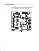
The printed circuit board plots for the SRC4192EVM are shown in Figure 4–3
through Figure 4–5. The PCB is a two–layer board, with most components
mounted on the top (or component) side. The power supply bypass capacitors
for U15 are mounted on the bottom (or solder) side of the PCB.
Figure 4–3. PCB Silkscreen, Top Layer