
Datasheet


The SRC4190, SRC4192, and SRC4193
1-3
Introduction
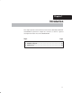
Figure 1–1. Functional Block Diagram for the SRC4192 and SRC4193
MODE[2:0]
IFMT[2:0]
OFMT[1:0]
OWL[1:0]
MUTE
BYPAS
LGRP
/RST
MUTE
BYPAS
/RST
/CS
CCLK
CDATA
LRCKI
BCKI
SDIN
LRCKO
BCKO
SDOUT
TDMI
/RDY
RATIO (SRC4193 only)
RCKI
Decimation
Filters
Direct
Down–Sampler
(SRC4193 only)
Re–Sampler
Interpolation
Filters
Rate
Estimator
LRCKI
LRCKO
Audio
Input
Port
Audio
Output
Port
Control
Logic
(SRC4192)
SPI and
Control Logic
(SRC4193)
MUX
Reference Clock
VDD
DGND
VIO
DGND
Power
REFCLK
REFCLK
f
sIN
16f
sIN
16f
sOUT
f
sOUT
f
sOUT
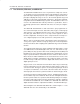
1.2 EVM Block Diagram
The block diagram for the SRC4192EVM is shown in Figure 1–2. The EVM in-
cludes buffered audio input and output ports that support I
2
S, Left Justified,
Right Justified, and TDM data formats. These ports may be connected to ex-
ternal receivers and transmitters, data converters, or digital signal processors.
An on–board 96kHz receiver is provided, as well as a 192kHz transmitter. The
receiver and transmitter provide for convenient connection to both test and
commercial audio equipment supporting AES3 or S/PDIF interfaces.
The SRC4192 and DIT4192 have their own external phase locked loop circuits
for on–board clock generation. External clock inputs are also available and
provide for additional flexibility. The EVM is configured using on–board
switches and jumpers, in addition to a buffered host port, which supports the
SRC4193 SPI interface. A single +5 volt power supply is all that is needed to
power the EVM. A +3.3 volt supply is derived from the +5 volt supply using an
on–board voltage regulator.