
Datasheet


V
DD2
V
DD2 V
DD2
V
DD2
S
REF
G
REF
V
REF
D
REF
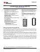
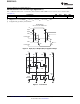
DUT
Test
Jig
Pulse
Generator
150 150 150200
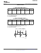
D1 . . . D8
S1 . . . S8
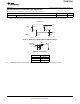
V
V
V
V
V
V
V
t
I
M
M
M
M
M
M
PHL
t
PLH
t
PHL0
t
PHL1
t
PLH0
t
PLH1
GND
V
DD2
V
DD2
V
OL
V
OL
Input
Low-to-High
Low-to-High
AC Waveforms
Vm = 1.5 V, V
IN
= GND to 3 V
SN74GTL2003
SCDS305A –FEBRUARY 2011–REVISED MARCH 2013
www.ti.com
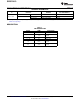
AC Characteristics for Translator-Type Applications
(1)
V
REF
= 1.365 V to 1.635 V, V
DD1
= 3 V to 3.6 V, V
DD2
= 2.36 V to 2.64 V, GND = 0 V, t
r
= t
f
≤ 3 ns, T
amb
= –40°C to 85°C
(see Figure 6)
PARAMETER MIN TYP
(2)
MAX UNIT
t
PLH
(3)
Propagation delay (Sn to Dn, Dn to Sn) 0.5 1.5 5.5 ns
(1) C
ON(max)
of 30 pF and a C
OFF(max)
of 15 pF is specified by design.
(2) All typical values are measured at V
DD1
= 3.3 V, V
DD2
= 2.5 V, V
REF
= 1.5 V and T
amb
= 25°C.
(3) Propagation delay specified by characterization.
Figure 2. Input (Sn) to Output (Dn) Propagation Delays
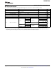
Figure 3. Load Circuit
6 Submit Documentation Feedback Copyright © 2011–2013, Texas Instruments Incorporated
Product Folder Links: SN74GTL2003