
Datasheet
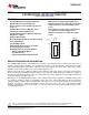

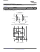

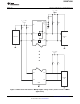

SN74GTL2003
SCDS305A –FEBRUARY 2011–REVISED MARCH 2013
www.ti.com
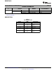
Absolute Maximum Ratings
(1)(2)(3)
over operating free-air temperature range (unless otherwise noted)
MIN MAX UNIT
V
SREF
DC source reference voltage –0.5 7 V
V
DREF
DC drain reference voltage –0.5 7 V
V
GREF
DC gate reference voltage –0.5 7 V
V
Sn
DC voltage port Sn –0.5 7 V
V
Dn
DC voltage port Dn –0.5 7 V
I
REFK
DC diode current on reference pins V
I
< 0 V –50 mA
I
SK
DC diode current port Sn V
I
< 0V –50 mA
I
DK
DC diode current port Dn V
I
< 0 V –50 mA
I
MAX
DC clamp current per channel Channel is ON state ±128 mA
θ
JA
Package thermal impedance 88 ºC/W
T
stg
Storage temperature range –65 150 °C
(1) Stresses beyond those listed under "absolute maximum ratings" may cause permanent damage to the device. These are stress ratings
only, and functional operation of the device at these or any other conditions beyond those indicated under "recommended operating
conditions" is not implied. Exposure to absolute-maximum-rated conditions for extended periods may affect device reliability.
(2) The performance capability of a high-performance integrated circuit in conjunction with its thermal environment can create junction
temperatures that are detrimental to reliability. The maximum junction temperature of this integrated circuit should not exceed 150°C.
(3) The input and output negative voltage ratings may be exceeded if the input and output clamp current ratings are observed.
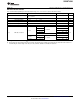
Recommended Operating Conditions
(1)
MIN MAX UNIT
V
I/O
Input/output voltage (Sn, Dn) 0 5.5 V
V
SREF
DC source reference voltage
(1)
0 5.5 V
V
DREF
DC drain reference voltage 0 5.5 V
V
GREF
DC gate reference voltage 0 5.5 V
I
PASS
Pass transistor current 64 mA
T
AMB
Operating ambient temperature range (in free air) –40 85 ºC
(1) V
SREF
= V
DREF
– 1.5 V for best results in level-shifting applications.
4 Submit Documentation Feedback Copyright © 2011–2013, Texas Instruments Incorporated
Product Folder Links: SN74GTL2003