
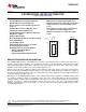
Datasheet


S
REF
D
REF
G
REF
SW
SW
GTL2003
D1
S1
D2
S2
Sn
GND
Dn
V = 1.8V
REF
200K Ω
CPU I/O
Chipset
I/O
V = 5 V
DPU
SN74GTL2003
SCDS305A –FEBRUARY 2011–REVISED MARCH 2013
www.ti.com
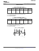
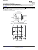
Unidirectional Down Translation
For unidirectional clamping (higher voltage to lower voltage), the G
REF
input must be connected to D
REF
and both
pins pulled to the higher-side V
CC
through a pullup resistor (typically 200 kW). A filter capacitor on D
REF
is
recommended. Pullup resistors are required if the chipset I/Os are open drain. The opposite side of the reference
transistor (S
REF
) is connected to the processor core power-supply voltage. When D
REF
is connected through a
200-kW resistor to a 3.3-V to 5.5-V V
CC
supply and S
REF
is set between 1 V to V
CC
– 1.5 V, the output of each Sn
has a maximum output voltage equal to S
REF
.
Figure 7. Unidirectional Down Translation to Protect Low-Voltage Processor Pins
10 Submit Documentation Feedback Copyright © 2011–2013, Texas Instruments Incorporated
Product Folder Links: SN74GTL2003