
Datasheet

www.ti.com
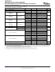
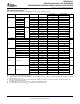
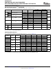
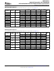
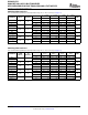
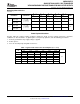
Absolute Maximum Ratings
(1)
SN74AVCH1T45
SINGLE-BIT DUAL-SUPPLY BUS TRANSCEIVER
WITH CONFIGURABLE VOLTAGE TRANSLATION AND 3-STATE OUTPUTS
SCES598D – JULY 2004 – REVISED JANUARY 2008
over operating free-air temperature range (unless otherwise noted)
MIN MAX UNIT
V
CCA
Supply voltage range – 0.5 4.6 V
V
CCB
I/O ports (A port) – 0.5 4.6
V
I
Input voltage range
(2)
I/O ports (B port) – 0.5 4.6 V
Control inputs – 0.5 4.6
A port – 0.5 4.6
Voltage range applied to any output in the high-impedance or
V
O
V
power-off state
(2)
B port – 0.5 4.6
A port – 0.5 V
CCA
+ 0.5
V
O
Voltage range applied to any output in the high or low state
(2) (3)
V
B port – 0.5 V
CCB
+ 0.5
I
IK
Input clamp current V
I
< 0 – 50 mA
I
OK
Output clamp current V
O
< 0 – 50 mA
I
O
Continuous output current ± 50 mA
Continuous current through V
CCA
, V
CCB
, or GND ± 100 mA
DBV package 165
θ
JA
Package thermal impedance
(4)
DCK package 259 ° C/W
YZP package 123
T
stg
Storage temperature range – 65 150 ° C
(1) Stresses beyond those listed under "absolute maximum ratings" may cause permanent damage to the device. These are stress ratings
only, and functional operation of the device at these or any other conditions beyond those indicated under "recommended operating
conditions" is not implied. Exposure to absolute-maximum-rated conditions for extended periods may affect device reliability.
(2) The input voltage and output negative-voltage ratings may be exceeded if the input and output current ratings are observed.
(3) The output positive-voltage rating may be exceeded up to 4.6 V maximum if the output current rating is observed.
(4) The package thermal impedance is calculated in accordance with JESD 51-7.
Copyright © 2004 – 2008, Texas Instruments Incorporated Submit Documentation Feedback 3
Product Folder Link(s): SN74AVCH1T45