
Datasheet


Table Of Contents
- FEATURES
- DESCRIPTION/ORDERING INFORMATION
- DESCRIPTION/ORDERING INFORMATION (CONTINUED)
- Absolute Maximum Ratings
- Recommended Operating Conditions
- Electrical Characteristics
- Switching Characteristics
- Switching Characteristics
- Switching Characteristics
- Switching Characteristics
- Switching Characteristics
- Operating Characteristics
- TYPICAL CHARACTERISTICS
- Typical Propagation Delay (A to B) vs Load CapacitanceTA = 25C, VCCA = 1.2 V
- Typical Propagation Delay (A to B) vs Load CapacitanceTA = 25C, VCCA = 1.5 V
- Typical Propagation Delay (A to B) vs Load CapacitanceTA = 25C, VCCA = 1.8 V
- Typical Propagation Delay (A to B) vs Load CapacitanceTA = 25C, VCCA = 2.5 V
- Typical Propagation Delay (A to B) vs Load CapacitanceTA = 25C, VCCA = 3.3 V
- PARAMETER MEASUREMENT INFORMATION
www.ti.com
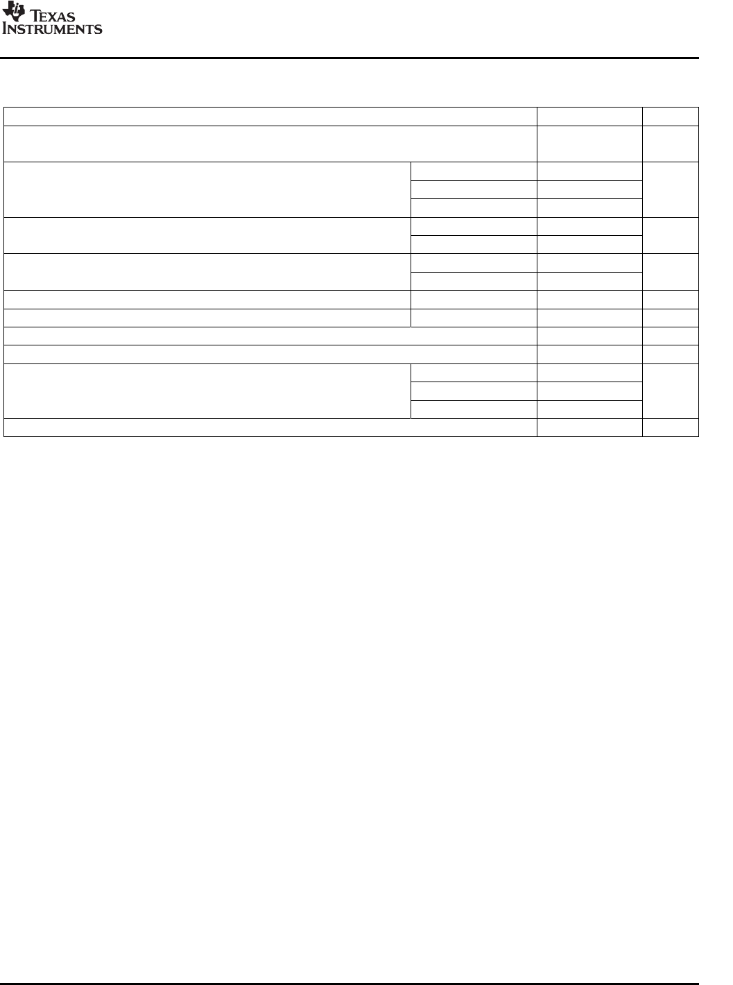
Absolute Maximum Ratings
(1)
SN74AVC8T245
8-BIT DUAL-SUPPLY BUS TRANSCEIVER
WITH CONFIGURABLE VOLTAGE TRANSLATION AND 3-STATE OUTPUTS
SCES517H – DECEMBER 2003 – REVISED FEBRUARY 2007
over operating free-air temperature range (unless otherwise noted)
MIN MAX UNIT
V
CCA
Supply voltage range –0.5 4.6 V
V
CCB
I/O ports (A port) –0.5 4.6
V
I
Input voltage range
(2)
I/O ports (B port) –0.5 4.6 V
Control inputs –0.5 4.6
A port –0.5 4.6
Voltage range applied to any output
V
O
V
in the high-impedance or power-off state
(2)
B port –0.5 4.6
A port –0.5 V
CCA
+ 0.5
V
O
Voltage range applied to any output in the high or low state
(2) (3)
V
B port –0.5 V
CCB
+ 0.5
I
IK
Input clamp current V
I
< 0 –50 mA
I
OK
Output clamp current V
O
< 0 –50 mA
I
O
Continuous output current ± 50 mA
Continuous current through V
CCA
, V
CCB
, or GND ± 100 mA
DGV package 86
θ
JA
Package thermal impedance
(4)
PW package 88 ° C/W
RHL package 43
T
stg
Storage temperature range –65 150 ° C
(1) Stresses beyond those listed under "absolute maximum ratings" may cause permanent damage to the device. These are stress ratings
only, and functional operation of the device at these or any other conditions beyond those indicated under "recommended operating
conditions" is not implied. Exposure to absolute-maximum-rated conditions for extended periods may affect device reliability.
(2) The input voltage and output negative-voltage ratings may be exceeded if the input and output current ratings are observed.
(3) The output positive-voltage rating may be exceeded up to 4.6 V maximum if the output current rating is observed.
(4) The package thermal impedance is calculated in accordance with JESD 51-7.
3
Submit Documentation Feedback