
Datasheet


Table Of Contents
- FEATURES
- DESCRIPTION/ORDERING INFORMATION
- DESCRIPTION/ORDERING INFORMATION (CONTINUED)
- Absolute Maximum Ratings
- Recommended Operating Conditions
- Electrical Characteristics
- Switching Characteristics
- Switching Characteristics
- Switching Characteristics
- Switching Characteristics
- Switching Characteristics
- Operating Characteristics
- TYPICAL CHARACTERISTICS
- Typical Propagation Delay (A to B) vs Load CapacitanceTA = 25C, VCCA = 1.2 V
- Typical Propagation Delay (A to B) vs Load CapacitanceTA = 25C, VCCA = 1.5 V
- Typical Propagation Delay (A to B) vs Load CapacitanceTA = 25C, VCCA = 1.8 V
- Typical Propagation Delay (A to B) vs Load CapacitanceTA = 25C, VCCA = 2.5 V
- Typical Propagation Delay (A to B) vs Load CapacitanceTA = 25C, VCCA = 3.3 V
- PARAMETER MEASUREMENT INFORMATION
www.ti.com
DESCRIPTION/ORDERING INFORMATION (CONTINUED)
DIR
OE
A1
B1
To Seven Other Channels
2
3
22
21
SN74AVC8T245
8-BIT DUAL-SUPPLY BUS TRANSCEIVER
WITH CONFIGURABLE VOLTAGE TRANSLATION AND 3-STATE OUTPUTS
SCES517H – DECEMBER 2003 – REVISED FEBRUARY 2007
The SN74AVC8T245 is designed for asynchronous communication between data buses. The device transmits
data from the A bus to the B bus or from the B bus to the A bus, depending on the logic level at the
direction-control (DIR) input. The output-enable ( OE) input can be used to disable the outputs so the buses are
effectively isolated.
The SN74AVC8T245 is designed so the control pins (DIR and OE) are supplied by V
CCA
.
The SN74AVC8T245 solution is compatible with a single-supply system and can be replaced later with a '245
function, with minimal printed circuit board redesign.
This device is fully specified for partial-power-down applications using I
off
. The I
off
circuitry disables the outputs,
preventing damaging current backflow through the device when it is powered down.
The V
CC
isolation feature ensures that if either V
CC
input is at GND, both ports are in the high-impedance state.
To ensure the high-impedance state during power up or power down, OE shall be tied to V
CC
through a pullup
resistor; the minimum value of the resistor is determined by the current-sinking capability of the driver.
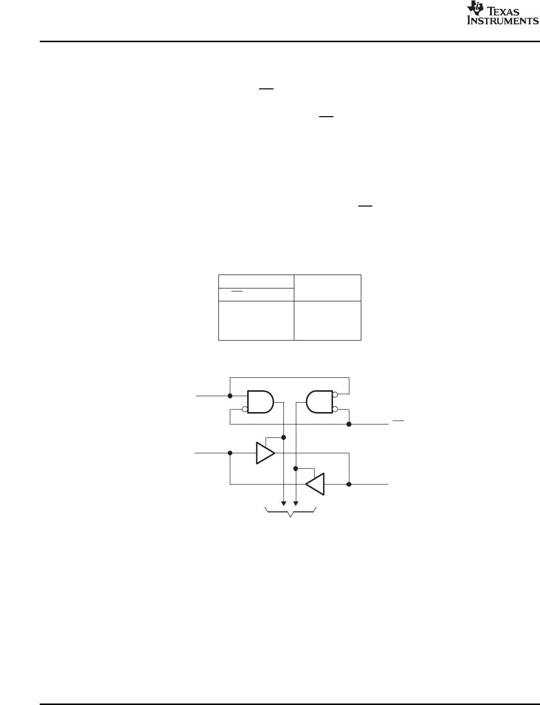
FUNCTION TABLE
(each 8-bit section)
INPUTS
OPERATION
OE DIR
L L B data to A bus
L H A data to B bus
H X All outputs Hi-Z
LOGIC DIAGRAM (POSITIVE LOGIC)
2
Submit Documentation Feedback